

Question
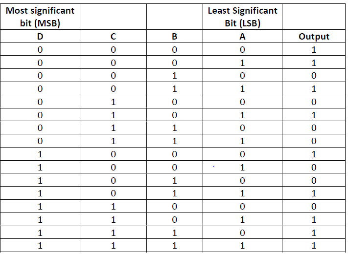
In this part, your aim is to verify the design method used for designing the combinational logic digital circuit. The truth table for a four-input
In this part, your aim is to verify the design method used for designing the combinational logic digital circuit. The truth table for a four-input digital combinational logic circuit is shown below. Draw the resultant circuit using any logic gates. The input of the logic gates cannot be more than two. Then simulate the circuit in Multisim. Use the Karnaugh Map (K-Map) method to find the simplest combinational digital circuit that will implement this truth table. Then draw the resultant circuit using any logic gates. The input of the logic gates cannot be more than two. Then simulate the circuit in Multisim and compare the outputs from the two methods and comment on the results (the K-Map you developed, and the Multisim output). What are the applications of the circuit (what can you use it for)?
please solve all part
Most significant bit (MSB) D C B Least Significant Bit (LSB) 0 1 0 0 0 0 Output 1 1 0 0 0 0 1 0 0 0 1 1 1 0 0 1 0 0 1 0 0 1 0 0 1 1 1 0 1 0 0 1 0 1 0 1 0 1 O 1 0 0 0 1 1 1 1 0 1 1 0 0 1 1 O 1 1 1 1 1 1 1 1 0 1 0 1 0 1 1 1 1Step by Step Solution
There are 3 Steps involved in it
Step: 1

Get Instant Access to Expert-Tailored Solutions
See step-by-step solutions with expert insights and AI powered tools for academic success
Step: 2

Step: 3
Ace Your Homework with AI
Get the answers you need in no time with our AI-driven, step-by-step assistance
Get Started
Database Benchmarking And Stress Testing An Evidence Based Approach To Decisions On Architecture And Technology
Authors: Bert Scalzo
1st Edition
148424009X, 978-1484240090