Just the code in VHDL, no need for anything else
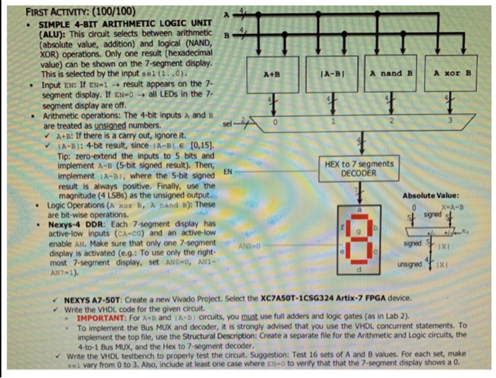
FIRST ACTIVITY: (100/100) SIMPLE 4-BIT ARITHMETIC LOGIC UNIT (ALU): This dirauit selects between arithmetic B (absolute value, addition) and logical (NAND XOR) operations. Only one result (hexadecimal value) can be shown on the 7-segment display This is selected by the input sel (1..0). A+B IA-BI | | A nand B| | A xor B Input EN: If EN-1 result appears on the 7- segment display. If EN-O, all LEDs in the 7- segment display are off Arithmetic operations: The 4-bit inputs A and B are treated as unsigned numbers sel A+B: If there is a carry out, ignore it IA-BI:4-bit result, since IA-BIE [0,15) Tip: zero-extend the inputs to 5 bits and implement A-B (5-bit signed result). Then, HEX to 7 segments DECODER implement IA-BI, where the 5-bit signed E result is always positive. Finally, use the magnitude (4 LSBs) as the unsigned output. Logic Operations (A xor B, A nand B): These Absolute Value: are bit-wise operations Nexys-4 DDR: Each 7-segment display has active-low inputs (CA-ca) and an active-low enable AN. Make sure that only one 7-segmentANO0 signed x display is activated (e.g.: To use only the right- most 7-segment display, set ANO-O, AN1 unsigned AN7-1). NEXYS A7-SOT: Create a new Vivado Project. Select the XC7ASOT-1CSG324 Artix-7 FPGA device. write the VHDL code for the given circuit. IMPORTANT: For A+B and IA-BI circuits, you must use full adders and logic gates (as in Lab 2). To implement the Bus MUX and decoder, it is strongly advised that you use the VHDL concurrent statements. To implement the top file, use the Structural Description: Create a separate file for the Arithmetic and Logic circuits, the 4-to-1 Bus Mux, and the Hex to 7-segment decoder v' Write the VHDL testbench to properly test the circuit. Suggestion: Test 16 sets of A and B values. For each set, make from 0 to 3. Also, include at least one case where ENo to verify that that the 7-segment display shows a o