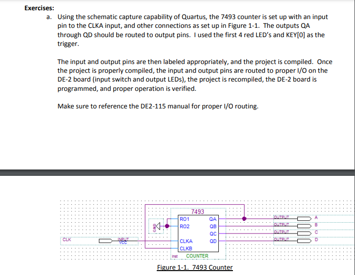
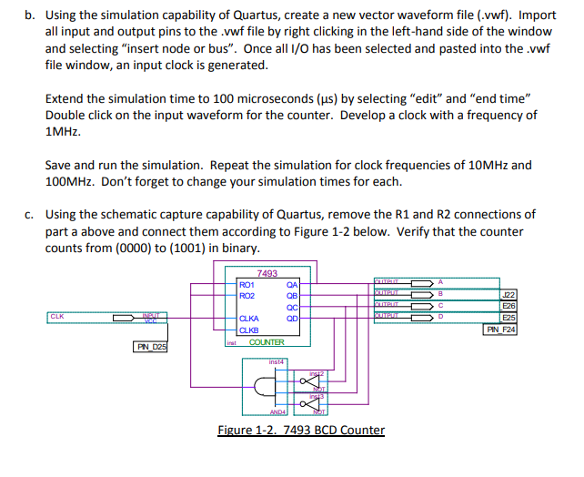
Lab 1 - Pre-Lab PURPOSE: To become familiar with binary numbers, simulation tools, basic test procedures, and the DE-2 board. PRE-LAB READINGS AND EXERCISES: Prior to the lab period, perform the following readings and exercises. Reading: Review information on binary numbers, number bases, and counting in the ECE 215 text Book. Review experiment 11-1 in the text book. Review the manuals for the DE2-115 board. . Review the Quartus tutorial and the Quartus Il manual. Background: This experiment is conducted during the first two laboratory periods. The basic element used in this experiment is a four bit binary counter, the 7493. The 7493 consists of a one-bit counter (or flip-flop) and a three-bit counter in the same package. Input A is the input to the one-bit counter and input B is the input to the three bit counter. Connecting output QA to input B creates a four-bit counter. Whenever the input of the counter is pulsed, the outputs assume a binary count which is one greater than the previous output. The counter also has two reset inputs, R1 and R2. The reset inputs are used to reset both the 3-bit counter and 1-bit counter to zero, regardless of the current output. Later in the course, we will experiment with the design of binary counters. However, for this experiment, we learn something about their behavior and learn to conduct measurements of digital circuits. This experiment repeats the above experiment using the Quartus design software and the Field Programmable Gate Array on the DE-2 development board. We will use the schematic capture feature of Quartus to enter our designs, the waveform simulation capability to test the design in simulation, and the DE-2 board for implementation. Exercises: a. Using the schematic capture capability of Quartus, the 7493 counter is set up with an input pin to the CLKA input, and other connections as set up in Figure 1-1. The outputs QA through QD should be routed to output pins. I used the first 4 red LED's and KEY[O] as the trigger The input and output pins are then labeled appropriately, and the project is compiled. Once the project is properly compiled, the input and output pins are routed to proper 1/0 on the DE-2 board (input switch and output LEDs), the project is recompiled, the DE-2 board is programmed, and proper operation is verified. Make sure to reference the DE2-115 manual for proper 1/0 routing. om 7493 RO1 QA ROZ QB QC CLKA QD CLKB Inst COUNTER CLK vee FOLTOUT D Figure 1-1. 7493 Counter b. Using the simulation capability of Quartus, create a new vector waveform file (vwf). Import all input and output pins to the .vwf file by right clicking in the left-hand side of the window and selecting "insert node or bus". Once all 1/0 has been selected and pasted into the vwf file window, an input clock is generated. Extend the simulation time to 100 microseconds (us) by selecting "edit" and "end time" Double click on the input waveform for the counter. Develop a clock with a frequency of 1MHz. Save and run the simulation. Repeat the simulation for clock frequencies of 10MHz and 100MHz. Don't forget to change your simulation times for each. C. Using the schematic capture capability of Quartus, remove the R1 and R2 connections of part a above and connect them according to Figure 1-2 below. Verify that the counter counts from (0000) to (1001) in binary. AUTE 7493 RO1 QA RO2 QC CLKA QD CLKB COUNTER 122 E26 E25 PIN F24 CLK ver PN D25 Inst2 NAT ing AND4 Figure 1-2. 7493 BCD Counter Lab 1 - Pre-Lab PURPOSE: To become familiar with binary numbers, simulation tools, basic test procedures, and the DE-2 board. PRE-LAB READINGS AND EXERCISES: Prior to the lab period, perform the following readings and exercises. Reading: Review information on binary numbers, number bases, and counting in the ECE 215 text Book. Review experiment 11-1 in the text book. Review the manuals for the DE2-115 board. . Review the Quartus tutorial and the Quartus Il manual. Background: This experiment is conducted during the first two laboratory periods. The basic element used in this experiment is a four bit binary counter, the 7493. The 7493 consists of a one-bit counter (or flip-flop) and a three-bit counter in the same package. Input A is the input to the one-bit counter and input B is the input to the three bit counter. Connecting output QA to input B creates a four-bit counter. Whenever the input of the counter is pulsed, the outputs assume a binary count which is one greater than the previous output. The counter also has two reset inputs, R1 and R2. The reset inputs are used to reset both the 3-bit counter and 1-bit counter to zero, regardless of the current output. Later in the course, we will experiment with the design of binary counters. However, for this experiment, we learn something about their behavior and learn to conduct measurements of digital circuits. This experiment repeats the above experiment using the Quartus design software and the Field Programmable Gate Array on the DE-2 development board. We will use the schematic capture feature of Quartus to enter our designs, the waveform simulation capability to test the design in simulation, and the DE-2 board for implementation. Exercises: a. Using the schematic capture capability of Quartus, the 7493 counter is set up with an input pin to the CLKA input, and other connections as set up in Figure 1-1. The outputs QA through QD should be routed to output pins. I used the first 4 red LED's and KEY[O] as the trigger The input and output pins are then labeled appropriately, and the project is compiled. Once the project is properly compiled, the input and output pins are routed to proper 1/0 on the DE-2 board (input switch and output LEDs), the project is recompiled, the DE-2 board is programmed, and proper operation is verified. Make sure to reference the DE2-115 manual for proper 1/0 routing. om 7493 RO1 QA ROZ QB QC CLKA QD CLKB Inst COUNTER CLK vee FOLTOUT D Figure 1-1. 7493 Counter b. Using the simulation capability of Quartus, create a new vector waveform file (vwf). Import all input and output pins to the .vwf file by right clicking in the left-hand side of the window and selecting "insert node or bus". Once all 1/0 has been selected and pasted into the vwf file window, an input clock is generated. Extend the simulation time to 100 microseconds (us) by selecting "edit" and "end time" Double click on the input waveform for the counter. Develop a clock with a frequency of 1MHz. Save and run the simulation. Repeat the simulation for clock frequencies of 10MHz and 100MHz. Don't forget to change your simulation times for each. C. Using the schematic capture capability of Quartus, remove the R1 and R2 connections of part a above and connect them according to Figure 1-2 below. Verify that the counter counts from (0000) to (1001) in binary. AUTE 7493 RO1 QA RO2 QC CLKA QD CLKB COUNTER 122 E26 E25 PIN F24 CLK ver PN D25 Inst2 NAT ing AND4 Figure 1-2. 7493 BCD Counter