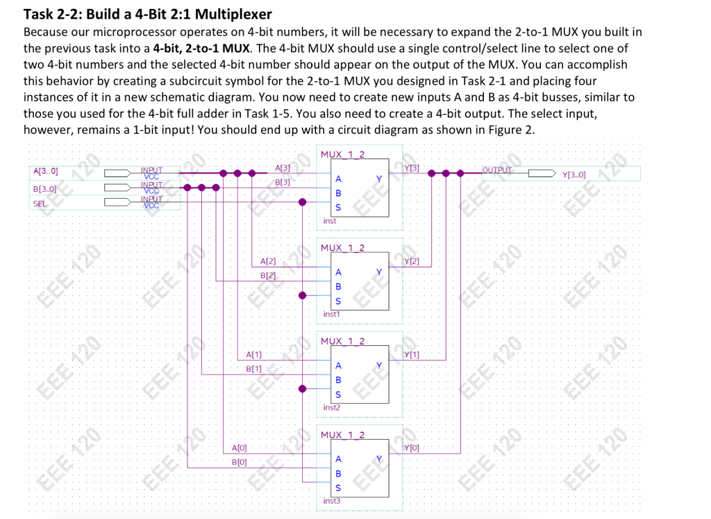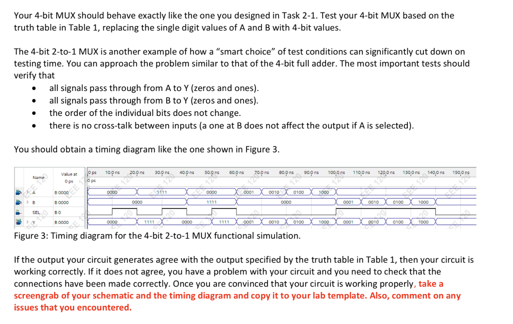


Lab 2: Multiplexers and Decoders Prerequisites: Before beginning this laboratory experiment you must be able to: Use Quartus Prime and the Waveform-based Modelsim simulator Interpret the operation of a Multiplexer and a Decoder. Equipment: Personal computer and Quartus Prime (Lite). Terasic DE10-Lite FPGA board. Objectives: In this laboratory exercise, you will build and debug combinational logic subcircuits that perform data routing and data display using Quartus and a Terasic DE10-Lite FPGA board Outcomes: When you have completed the tasks in this experiment you will be able to: Build and debug a simulation of a 2-to-1 multiplexer circuit. . Build and debug a simulation of a 4-bit, 2-to-1 multiplexer circuit. .Build and debug a simulation of a 4-to-16 decoder circuit. .Build and debug a simulation of a seven-segment display decoder circuit. Generate and upload a bitstream file to test the operation of the 4-bit adder on FPGA hardware using switches as inputs and seven-segment displays as indicators. Introduction In this laboratory exercise you will continue constructing modules that will eventually be used in assembling the microprocessor. Our concern in this laboratory exercise is with circuits that control the flow of data through our system (the multiplexer and decoder). You will eventually use the data-flow-control circuits you create in this lab exercise, a 4-bit 2-to-1 multiplexer and a 3-to-8 decoder, to make the microprocessor self-capable of routing data to appropriate locations as well as activate specific memory locations. You will also use a decoder to convert a set of binary values into digital signals that allow you to display the hexadecimal equivalent of the binary value on a seven-segment display. Task 2-2: Build a 4-Bit 2:1 Multiplexer Because our microprocessor operates on 4-bit numbers, it will be necessary to expand the 2-to-1 MUX you built in the previous task into a 4-bit, 2-to-1 MUX. The 4-bit MUX should use a single control/select line to select one of two 4-bit numbers and the selected 4-bit number should appear on the output of the MUX. You can accomplish this behavior by creating a subcircuit symbol for the 2-to-1 MUX you designed in Task 2-1 and placing four instances of it in a new schematic diagram. You now need to create new inputs A and B as 4-bit busses, similar to those you used for the 4-bit full adder in Task 1-5. You also need to create a 4-bit output. The select input however, remains a 1-bit input! You should end up with a circuit diagram as shown in Figure 2 MUX 3.01 B(3] B[3.0] A[2 MU A(1 MU AfOj Figure 2: Circuit schematic for a 4-bit 2-to-1 MUX. Your 4-bit MUX should behave exactly like the one you designed in Task 2-1. Test your 4-bit MUX based on the truth table in Table 1, replacing the single digit values of A and B with 4-bit values The 4-bit 2-to-1 MUX is another example of how a "smart choice" of test conditions can significantly cut down on testing time. You can approach the problem similar to that of the 4-bit full adder. The most important tests should verify that all signals pass through from A to Y (zeros and ones) all signals pass through from B to Y (zeros and ones) . the order of the individual bits does not change. . there is no cross-talk between inputs (a one at B does not affect the output if A is selected) You should obtain a timing diagram like the one shown in Figure 3 Value at ps ns 20.0ns 30.0ns 40.0 ns 50.0 ns ns 80.0ns 90.0ns 100.0 ns 110.0 ns 120.0ns 130.0 ns 140.0ns 150.0 ns 0 ps ps 0001 0010 0100 B 0000 B0000 B0 B 0000 0001 0010 0100 1000 SEL 0010 0100 1000 0001 0100 1000 Figure 3: Timing diagram for the 4-bit 2-to-1 MUX functional simulation If the output your circuit generates agree with the output specified by the truth table in Table 1, then your circuit is working correctly. If it does not agree, you have a problem with your circuit and you need to check that the connections have been made correctly. Once you are convinced that your circuit is working properly, take a screengrab of your schematic and the timing diagram and copy it to your lab template. Also, comment on any issues that you encountered
