

Answered step by step
Verified Expert Solution
Question
1 Approved Answer
Lab 3 Boolean Reduction Objectives: - Derive a truth table from a combinational logic circuit - Simplify a complex combinational circuit through Boolean reduction and
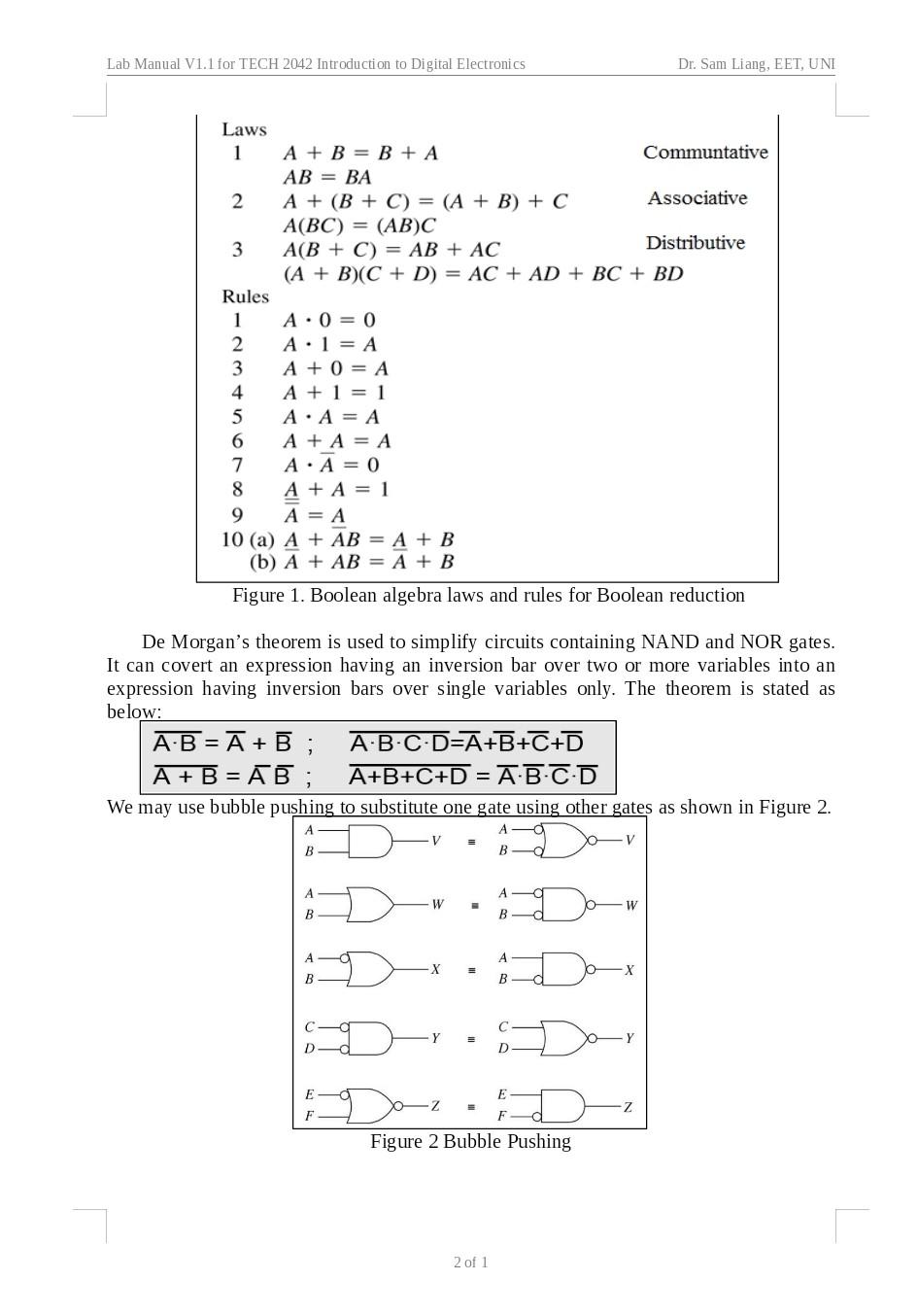
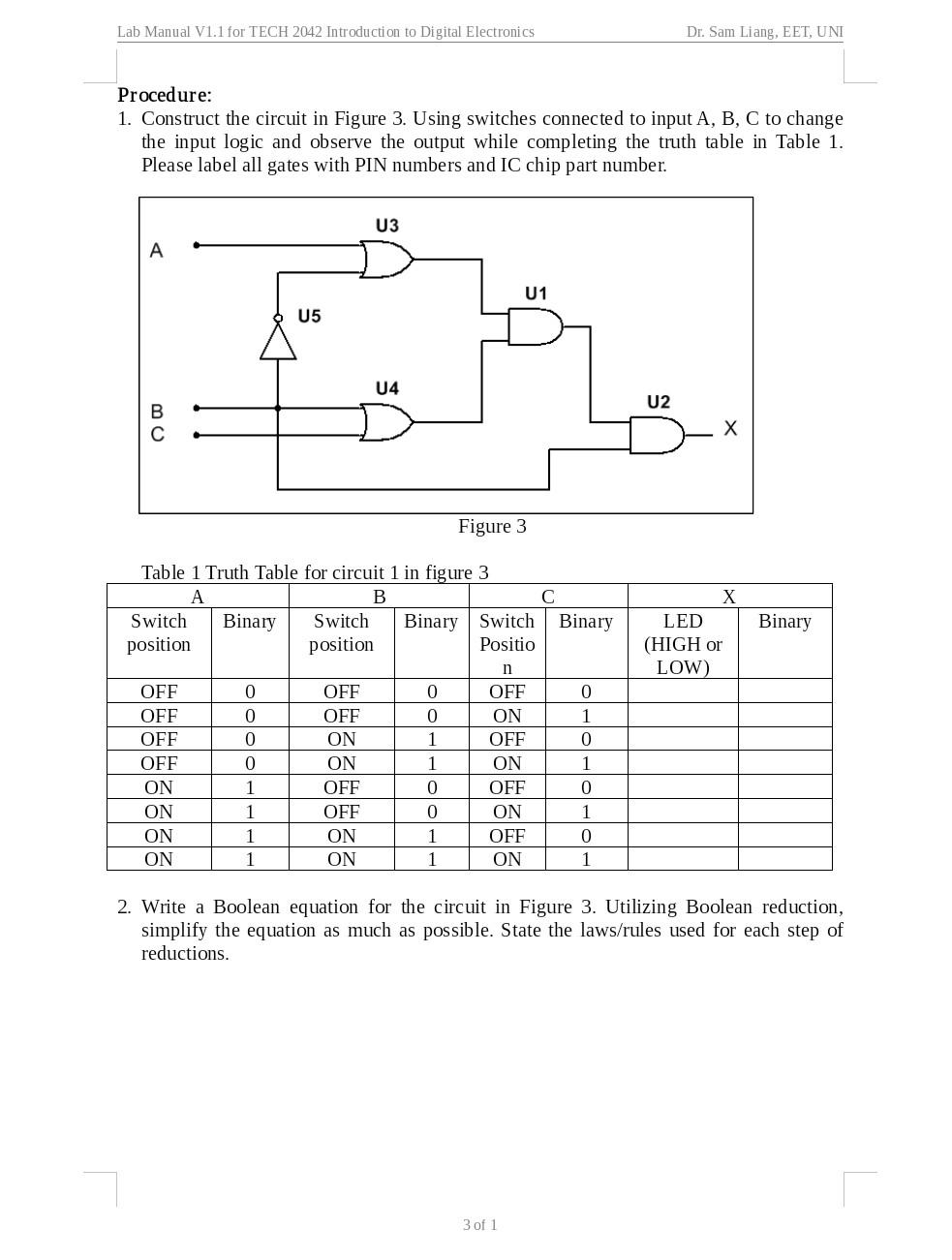
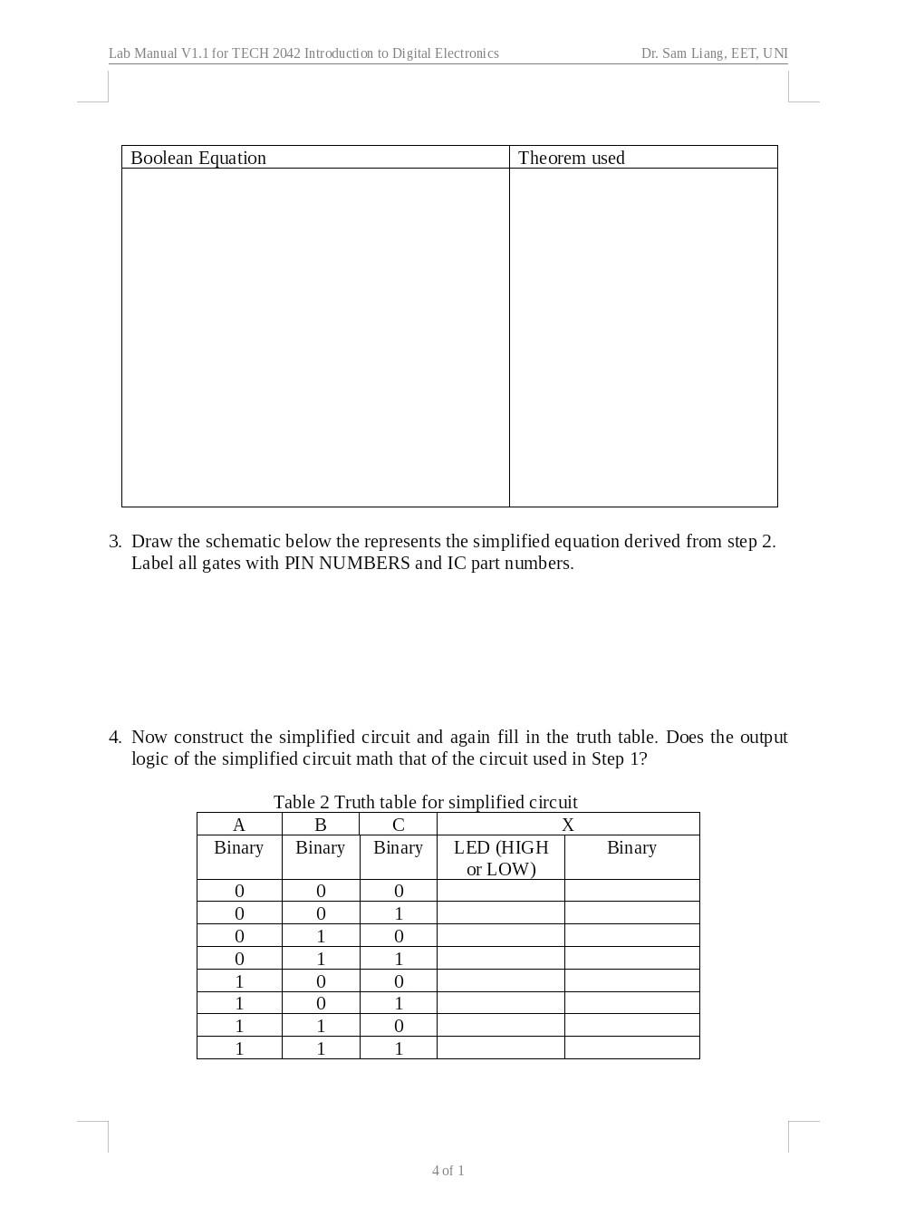
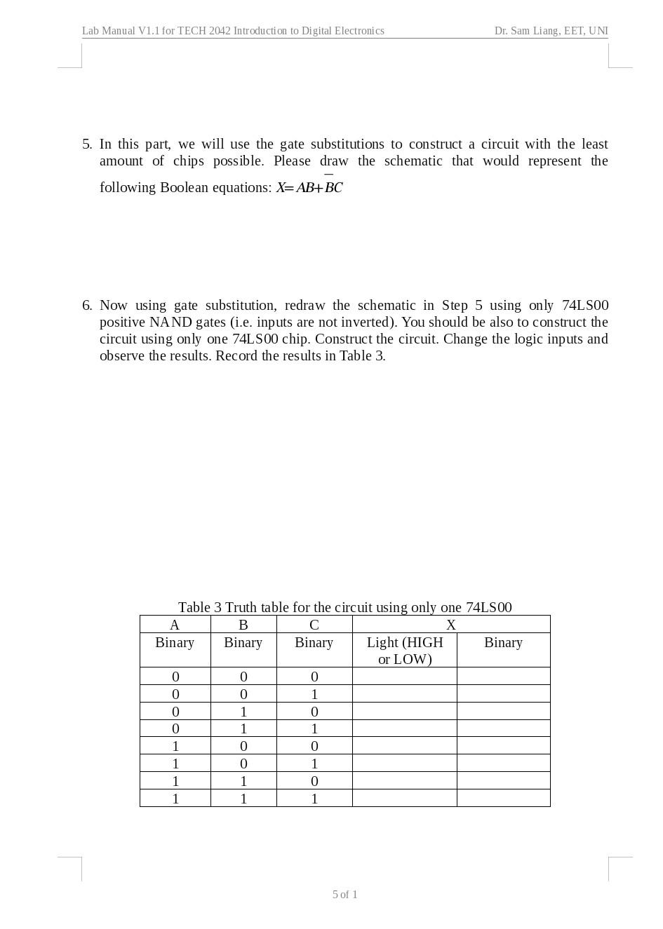
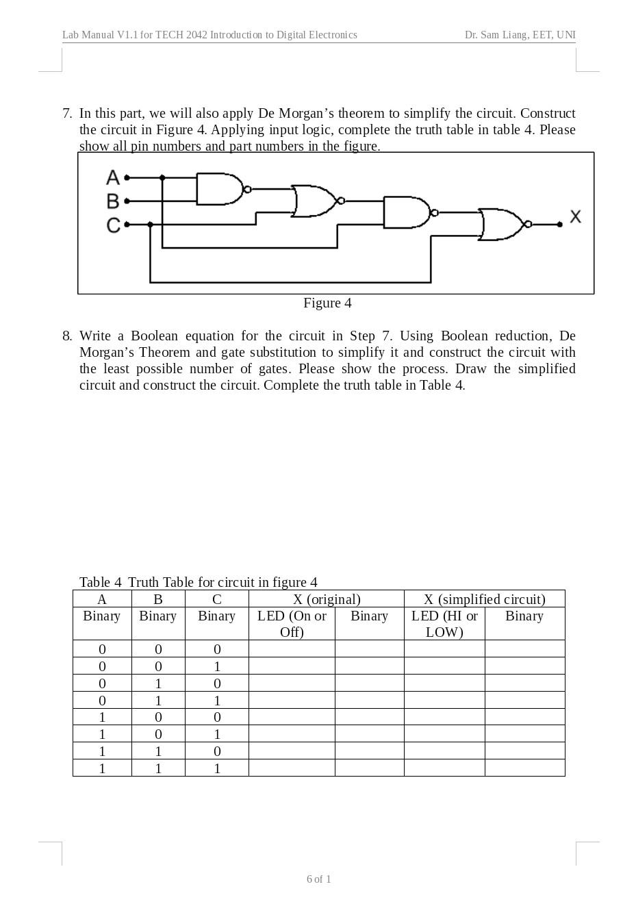
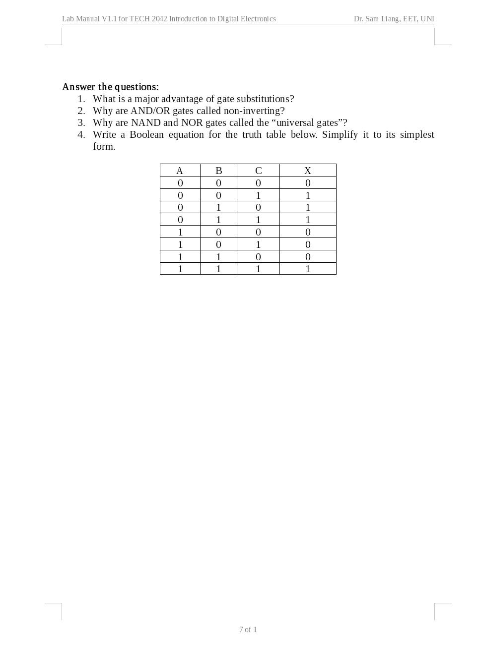
Lab 3 Boolean Reduction Objectives: - Derive a truth table from a combinational logic circuit - Simplify a complex combinational circuit through Boolean reduction and De Morgan's theory. - Design a circuit using least amount of chips using gate substitution. - Design a combinational logic circuit from a truth table. Equipment and Parts: +5V DC Supply Logic probe Lab Trainer or Proto Board (with LEDs and Switches) (1) 74LS08 quad 2 -input AND gate (1) 74LS32 quad 2-input OR gate (1) 74LS04 hex inverter (1) 74LS00 quad 2-input NAND gate (1) 74LS02 quad 2-input NOR gate Description: Combinational logic consists of two or more of the basic logic gates to perform a more complex function. The combinational logic is usually designed to satisfy a specific need. Boolean algebra and De Morgan's theory are useful tools to simplify the circuits to a simpler circuit to perform the same function. In this lab, we will construct the complex circuit and the simplified circuits, and compare the results. We will also learn to use the same type of gates to construct logic circuits to minimize the number of ICs used. Please refer to the chapter 5 in the textbook for Boolean reduction techniques. The Boolean algebra laws and rules are summarized in Figure 1. rigure 1 . boolean aggedra saws and rules ior boolean reauction De Morgan's theorem is used to simplify circuits containing NAND and NOR gates. It can covert an expression having an inversion bar over two or more variables into an expression having inversion bars over single variables only. The theorem is stated as below: AB=A+B;A+B=AB;ABCD=A+B+C+DA+B+C+D=ABCD We may use bubble pushing to substitute one gate using other gates as shown in Figure 2. Procedure: 1. Construct the circuit in Figure 3 . Using switches connected to input A, B, C to change the input logic and observe the output while completing the truth table in Table 1. Please label all gates with PIN numbers and IC chip part number. Table 1 Truth Table for circuit 1 in figure 3 2. Write a Boolean equation for the circuit in Figure 3. Utilizing Boolean reduction, simplify the equation as much as possible. State the laws/rules used for each step of reductions. 3. Draw the schematic below the represents the simplified equation derived from step 2. Label all gates with PIN NUMBERS and IC part numbers. 4. Now construct the simplified circuit and again fill in the truth table. Does the output logic of the simplified circuit math that of the circuit used in Step 1? 5. In this part, we will use the gate substitutions to construct a circuit with the least amount of chips possible. Please draw the schematic that would represent the following Boolean equations: X=AB+BC 6. Now using gate substitution, redraw the schematic in Step 5 using only 74LS00 positive NAND gates (i.e. inputs are not inverted). You should be also to construct the circuit using only one 74LS00 chip. Construct the circuit. Change the logic inputs and observe the results. Record the results in Table 3. Tahle 3 Truth tahle for the rircuit meino onlv nne 74TS 7. In this part, we will also apply De Morgan's theorem to simplify the circuit. Construct the circuit in Figure 4. Applying input logic, complete the truth table in table 4. Please show all pin numbers and part numbers in the figure. 8. Write a Boolean equation for the circuit in Step 7. Using Boolean reduction, De Morgan's Theorem and gate substitution to simplify it and construct the circuit with the least possible number of gates. Please show the process. Draw the simplified circuit and construct the circuit. Complete the truth table in Table 4. Tahlo Truth Tahla for rircuit in fioura Answer the questions: 1. What is a major advantage of gate substitutions? 2. Why are AND/OR gates called non-inverting? 3. Why are NAND and NOR gates called the "universal gates"? 4. Write a Boolean equation for the truth table below. Simplify it to its simplest form
Step by Step Solution
There are 3 Steps involved in it
Step: 1

Get Instant Access to Expert-Tailored Solutions
See step-by-step solutions with expert insights and AI powered tools for academic success
Step: 2

Step: 3
Ace Your Homework with AI
Get the answers you need in no time with our AI-driven, step-by-step assistance
Get Started
Mastering Real Time Analytics In Big Data A Comprehensive Guide For Everyone
Authors: Lennox Mark
1st Edition
B0CPTC9LY9, 979-8869045706