Lab 3 Sequential Logic Design


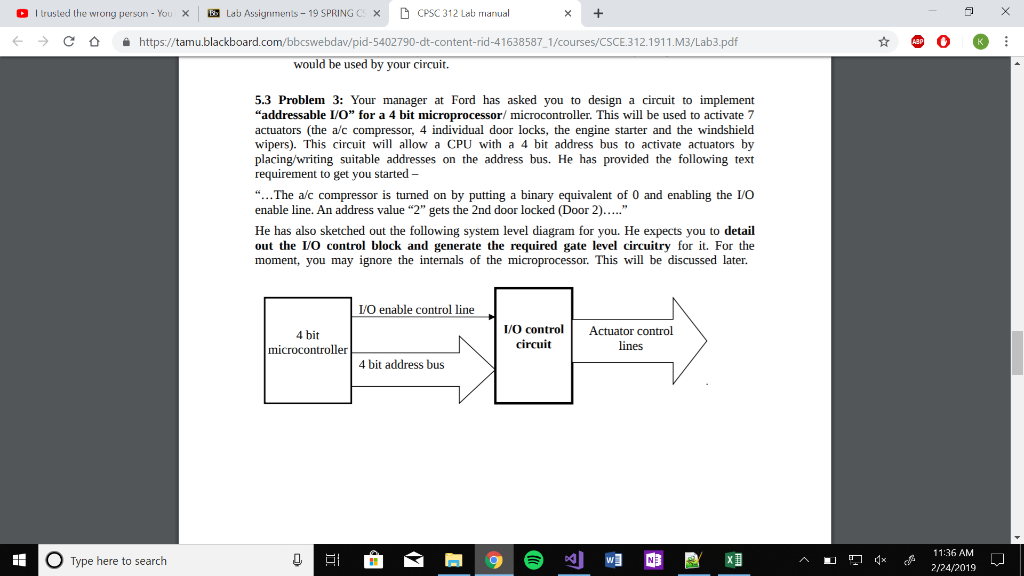
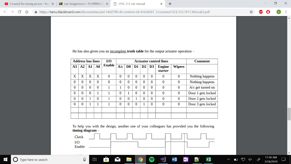
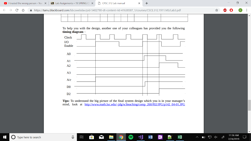
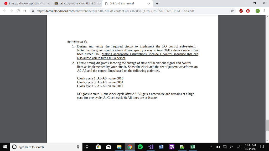
O l trusted lhe wrong person . You Lau Assignments-19 SPRING C: D CPSC 312 Lab manual https://tamu.blackboard.com/bbcswebdav/pid-5402790-dt-content-rid-41638587_1 312.1911.M3/Lab3.pdf would be used by your circuit 5.3 Problem 3: Your manager at Ford has asked you to design a circuit to implement "addressable LO" for a 4 bit microprocessor/ microcontroller. This will be used to activate7 actuators the a/c compressor, 4 individual door locks, the engine starter and the windshield wipers). This circuit will allow a CPU with a 4 bit address bus to activate actuators by placing/writing suitable addresses on the address bus. He has provided the following text requirement to get you started "...The a/c compressor is turned on by putting a binary equivalent of 0 and enabling the LIOo enable line. An address value "2" gets the 2nd door locked (Door 2)....." He has also sketched out the following system 1 out the IVO control block and generate the required gate level circuitry for it. For the moment, you may ignore the internals of the microprocessor. This will be discussed later. level diagram for you. He expects you to detail L/O enable control line /O contro Actuator control 4 bit microcontroller circuit 4 bit address bus 11:36 AM Type here to search 2/24/2019 O l trusted lhe wrong person . You Lau Assignments-19 SPRING C: D CPSC 312 Lab manual https://tamu.blackboard.com/bbcswebdav/pid-5402790-dt-content-rid-41638587_1 312.1911.M3/Lab3.pdf He has also given you an incomplete truth table for the output actuator operation - Address bus lines LIO Enable A/cDO D1 D2 D3 Engine Wipers Actuator control lines A3 A2 A1 A0 starter 0 Nothing happens 0 Nothing happens A/c get turned on 0 Door 1 gets locked 0 Door 2 gets locked 0 Door 3 gets locked 0 010 0 01 0 0 0 011 0 0 0 1 0 To help you with the design, another one of your colleagues has provided you the following timing diagram - Clock LVO Enable 11:36 AM Type here to search 2/24/2019 O l trusted lhe wrong person . You Lau Assignments-19 SPRING C: D CPSC 312 Lab manual https://tam ublackboard.com/bbcswebdav/pid-5402790-dt-content-rid-41638587-1/courses/CSCE.312.191 1.M3/Lab3.pdf To help you with the design, another one of your colleagues has provided you the following timing diagram - Clock LVO Enable A0 A1 A2 A3 A/c DO D2 Tips: To understand the big picture of the final system design which you is in your manager's mi 11:36 AM Type here to search 2/24/2019 O l trusted lhe wrong person . You Lau Assignments-19 SPRING C: D CPSC 312 Lab manual https://tamu.blackboard.com/bbcswebdav/pid-5402790-dt-content-rid-41638587_1 312.1911.M3/Lab3.pdf Activities to do- 1. Design and verify the required circuit to implement the I/O control sub-system. Note that the given specifications do not specify a way to turn OFF a device once it has been turned ON. Makin im 2. Create timing diagrams showing the change of state of the various signal and control lines as implemented by your circuit. Show the clock and the set of pattern waveforms on A0-A3 and the control lines based on the following activities. Clock cycle 1: A3-A0: value 0010 Clock cycle 3: A3-A0: value 0001 Clock cycle 5: A3-A0: value 0011 /O goes to state-1, one clock cycle after A3-A0 gets a new value and remains at a high state for one cycle. At Clock cycle 0; All lines are at 0 state 11:36 AM Type here to search 2/24/2019 O l trusted lhe wrong person . You Lau Assignments-19 SPRING C: D CPSC 312 Lab manual https://tamu.blackboard.com/bbcswebdav/pid-5402790-dt-content-rid-41638587_1 312.1911.M3/Lab3.pdf would be used by your circuit 5.3 Problem 3: Your manager at Ford has asked you to design a circuit to implement "addressable LO" for a 4 bit microprocessor/ microcontroller. This will be used to activate7 actuators the a/c compressor, 4 individual door locks, the engine starter and the windshield wipers). This circuit will allow a CPU with a 4 bit address bus to activate actuators by placing/writing suitable addresses on the address bus. He has provided the following text requirement to get you started "...The a/c compressor is turned on by putting a binary equivalent of 0 and enabling the LIOo enable line. An address value "2" gets the 2nd door locked (Door 2)....." He has also sketched out the following system 1 out the IVO control block and generate the required gate level circuitry for it. For the moment, you may ignore the internals of the microprocessor. This will be discussed later. level diagram for you. He expects you to detail L/O enable control line /O contro Actuator control 4 bit microcontroller circuit 4 bit address bus 11:36 AM Type here to search 2/24/2019 O l trusted lhe wrong person . You Lau Assignments-19 SPRING C: D CPSC 312 Lab manual https://tamu.blackboard.com/bbcswebdav/pid-5402790-dt-content-rid-41638587_1 312.1911.M3/Lab3.pdf He has also given you an incomplete truth table for the output actuator operation - Address bus lines LIO Enable A/cDO D1 D2 D3 Engine Wipers Actuator control lines A3 A2 A1 A0 starter 0 Nothing happens 0 Nothing happens A/c get turned on 0 Door 1 gets locked 0 Door 2 gets locked 0 Door 3 gets locked 0 010 0 01 0 0 0 011 0 0 0 1 0 To help you with the design, another one of your colleagues has provided you the following timing diagram - Clock LVO Enable 11:36 AM Type here to search 2/24/2019 O l trusted lhe wrong person . You Lau Assignments-19 SPRING C: D CPSC 312 Lab manual https://tam ublackboard.com/bbcswebdav/pid-5402790-dt-content-rid-41638587-1/courses/CSCE.312.191 1.M3/Lab3.pdf To help you with the design, another one of your colleagues has provided you the following timing diagram - Clock LVO Enable A0 A1 A2 A3 A/c DO D2 Tips: To understand the big picture of the final system design which you is in your manager's mi 11:36 AM Type here to search 2/24/2019 O l trusted lhe wrong person . You Lau Assignments-19 SPRING C: D CPSC 312 Lab manual https://tamu.blackboard.com/bbcswebdav/pid-5402790-dt-content-rid-41638587_1 312.1911.M3/Lab3.pdf Activities to do- 1. Design and verify the required circuit to implement the I/O control sub-system. Note that the given specifications do not specify a way to turn OFF a device once it has been turned ON. Makin im 2. Create timing diagrams showing the change of state of the various signal and control lines as implemented by your circuit. Show the clock and the set of pattern waveforms on A0-A3 and the control lines based on the following activities. Clock cycle 1: A3-A0: value 0010 Clock cycle 3: A3-A0: value 0001 Clock cycle 5: A3-A0: value 0011 /O goes to state-1, one clock cycle after A3-A0 gets a new value and remains at a high state for one cycle. At Clock cycle 0; All lines are at 0 state 11:36 AM Type here to search 2/24/2019
