Answered step by step
Verified Expert Solution
Question
1 Approved Answer
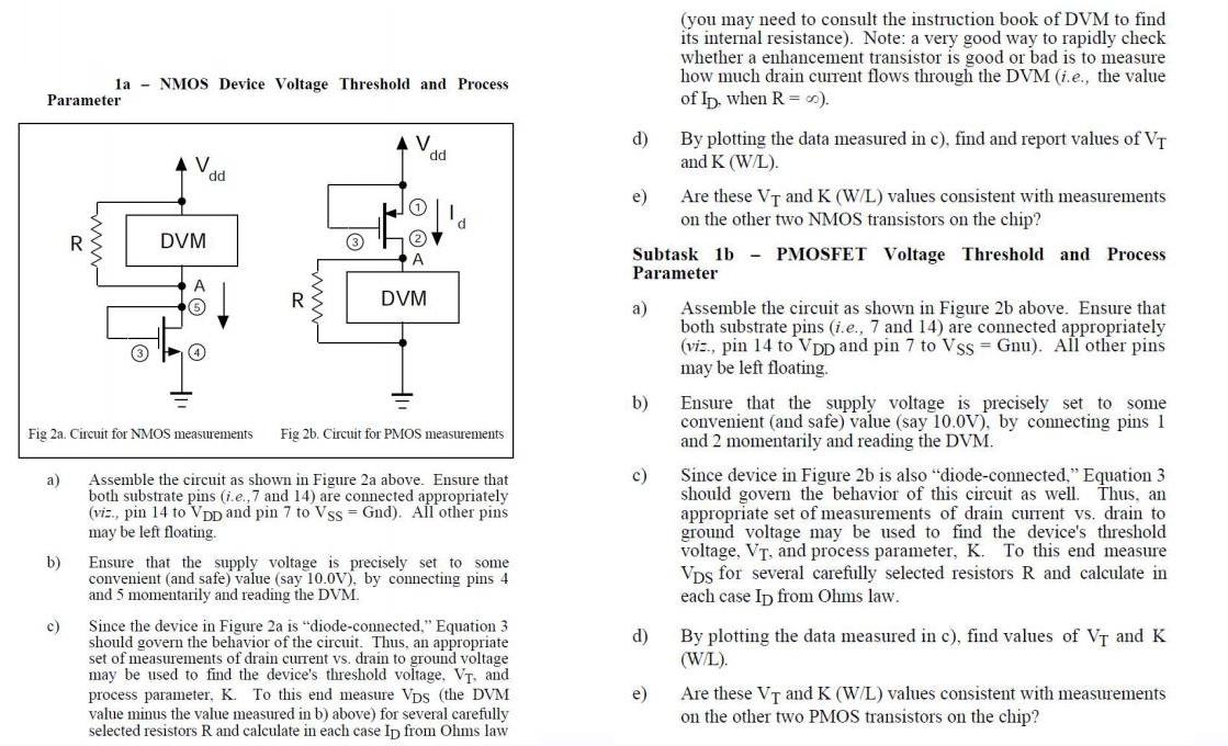
Parameter a) b) la NMOS Device Voltage Threshold and Process R c) V DVM dd 3 V. 1 A Fig 2a. Circuit for NMOS

Parameter a) b) la NMOS Device Voltage Threshold and Process R c) V DVM dd 3 V. 1 A Fig 2a. Circuit for NMOS measurements Fig 2b. Circuit for PMOS measurements DVM dd Assemble the circuit as shown in Figure 2a above. Ensure that both substrate pins (i.e.,7 and 14) are connected appropriately (viz., pin 14 to VDD and pin 7 to Vss = Gnd). All other pins may be left floating. Ensure that the supply voltage is precisely set to some convenient (and safe) value (say 10.0V), by connecting pins 4 and 5 momentarily and reading the DVM. Since the device in Figure 2a is "diode-connected." Equation 3 should govern the behavior of the circuit. Thus, an appropriate set of measurements of drain current vs. drain to ground voltage may be used to find the device's threshold voltage. VT, and process parameter, K. To this end measure Vps (the DVM value minus the value measured in b) above) for several carefully selected resistors R and calculate in each case Ip from Ohms law d) e) a) b) Subtask 1b - PMOSFET Voltage Threshold and Process Parameter c) (you may need to consult the instruction book of DVM to find its internal resistance). Note: a very good way to rapidly check whether a enhancement transistor is good or bad is to measure how much drain current flows through the DVM (i.e., the value of ID, when R= ). d) By plotting the data measured in c), find and report values of VT and K (W/L). Are these VT and K (W/L) values consistent with measurements on the other two NMOS transistors on the chip? Assemble the circuit as shown in Figure 2b above. Ensure that both substrate pins (i.e., 7 and 14) are connected appropriately (viz., pin 14 to VDD and pin 7 to Vss - Gnu). All other pins may be left floating. Ensure that the supply voltage is precisely set to some convenient (and safe) value (say 10.0V), by connecting pins 1 and 2 momentarily and reading the DVM. Since device in Figure 2b is also "diode-connected." Equation 3 should govern the behavior of this circuit as well. Thus, an appropriate set of measurements of drain current vs. drain to ground voltage may be used to find the device's threshold voltage, VT, and process parameter, K. To this end measure VDs for several carefully selected resistors R and calculate in each case ID from Ohms law. By plotting the data measured in c), find values of V and K (W/L). e) Are these VT and K (W/L) values consistent with measurements. on the other two PMOS transistors on the chip?
Step by Step Solution
★★★★★
3.46 Rating (162 Votes )
There are 3 Steps involved in it
Step: 1

Get Instant Access to Expert-Tailored Solutions
See step-by-step solutions with expert insights and AI powered tools for academic success
Step: 2

Step: 3

Ace Your Homework with AI
Get the answers you need in no time with our AI-driven, step-by-step assistance
Get Started


