Question
!!!!!!!!!!!!!!!!!!!!! MUST BE DONE IN THE SCHEME PROGRAMMING LANGUAGE !!!!!!!!!!!!!!!!!!!!!!!!!!!!!!!!!!!!!!!!!!!!!!!!!!!!!!!!!!!!!!!!!!!!!!!!!!!!!!!!!!!!!!!! !!!!!!!!!!!!!!!!!!!!! MUST BE DONE IN THE SCHEME PROGRAMMING LANGUAGE !!!!!!!!!!!!!!!!!!!!!!!!!!!!!!!!!!!!!!!!!!!!!!!!!!!!!!!!!!!!!!!!!!!!!!!!!!!!!!!!!!!!!!!! !!!!!!!!!!!!!!!!!!!!! MUST BE DONE IN


 !!!!!!!!!!!!!!!!!!!!! MUST BE DONE IN THE SCHEME PROGRAMMING LANGUAGE !!!!!!!!!!!!!!!!!!!!!!!!!!!!!!!!!!!!!!!!!!!!!!!!!!!!!!!!!!!!!!!!!!!!!!!!!!!!!!!!!!!!!!!!
!!!!!!!!!!!!!!!!!!!!! MUST BE DONE IN THE SCHEME PROGRAMMING LANGUAGE !!!!!!!!!!!!!!!!!!!!!!!!!!!!!!!!!!!!!!!!!!!!!!!!!!!!!!!!!!!!!!!!!!!!!!!!!!!!!!!!!!!!!!!!
!!!!!!!!!!!!!!!!!!!!! MUST BE DONE IN THE SCHEME PROGRAMMING LANGUAGE !!!!!!!!!!!!!!!!!!!!!!!!!!!!!!!!!!!!!!!!!!!!!!!!!!!!!!!!!!!!!!!!!!!!!!!!!!!!!!!!!!!!!!!!
!!!!!!!!!!!!!!!!!!!!! MUST BE DONE IN THE SCHEME PROGRAMMING LANGUAGE !!!!!!!!!!!!!!!!!!!!!!!!!!!!!!!!!!!!!!!!!!!!!!!!!!!!!!!!!!!!!!!!!!!!!!!!!!!!!!!!!!!!!!!!
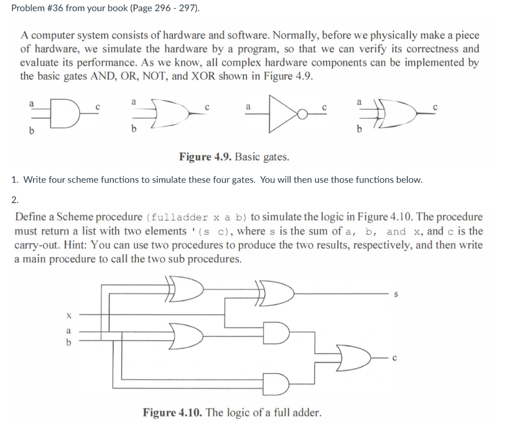
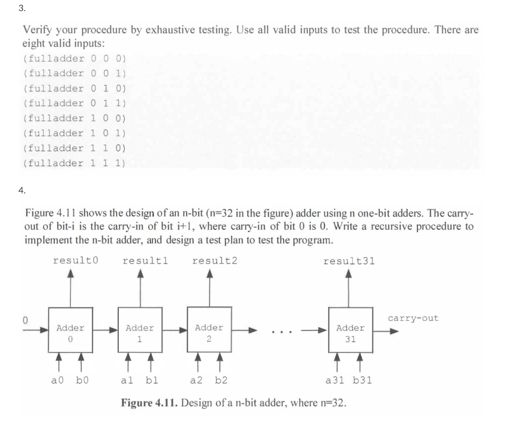
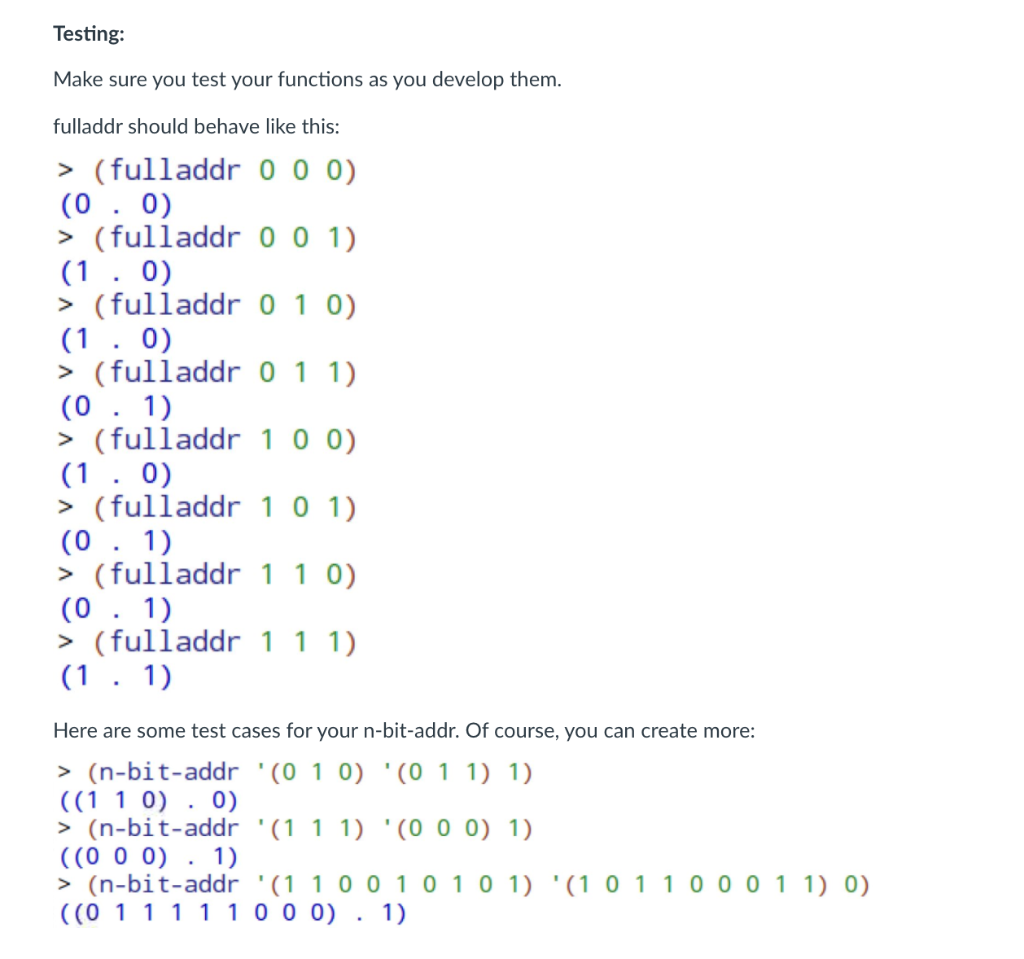
Problem #36 from your book (Page 296 - 297). A computer system consists of hardware and software. Normally, before we physically make a piece of hardware, we simulate the hardware by a program, so that we can verify its correctness and evaluate its performance. As we know, all complex hardware components can be implemented by the basic gates AND, OR, NOT, and XOR shown in Figure 4.9. a a a a Doo b b b Figure 4.9. Basic gates. 1. Write four scheme functions to simulate these four gates. You will then use those functions below. 2. Define a Scheme procedure (fulladder x a b) to simulate the logic in Figure 4.10. The procedure must return a list with two elements '(sc), where s is the sum of a, b, ar x, and c is the carry-out. Hint: You can use two procedures to produce the two results, respectively, and then write a main procedure to call the two sub procedures. X a b Figure 4.10. The logic of a full adder. 3. Verify your procedure by exhaustive testing. Use all valid inputs to test the procedure. There are eight valid inputs: (fulladder 0 0 0) (fulladder 001) (fulladder 0 1 0 (fulladder 0 1 1) (fulladder 1 00) (fulladder 1 O 1) (fulladder 1 1 0 (fulladder i 1 1) 4. Figure 4.11 shows the design of an n-bit (n=32 in the figure) adder using n one-bit adders. The carry- out of bit-i is the carry-in of bit i+1, where carry-in of bit 0 is 0. Write a recursive procedure to implement the n-bit adder, and design a test plan to test the program. resulto resulti result2 result31 0 carry-out Adder 0 Adder 1 Adder 2 Adder 31 A 1 al bi 0 bo a 2 b2 a 31 b31 Figure 4.11. Design of a n-bit adder, where n=32. Testing: Make sure you test your functions as you develop them. fulladdr should behave like this: > (fulladdr 0 0 0 (0.0 > (fulladdr 0 0 1) (1.0) > (fulladdr 0 1 0) (1 : 0) > (fulladdr 0 1 1) (0 : 1) > (fulladdr 100) (1 : 0) > (fulladdr 1 0 1) (0 : 1) > (fulladdr 1 10) (0.1) > (fulladdr 1 1 1) (1 . 1) Here are some test cases for your n-bit-addr. Of course, you can create more: > (n-bit-addr '(0 10) '(0 1 1) 1) ((1 1 0 : 0) > (n-bit-addr '(1 1 1) '(0 0 0) 1) ((0 0 0) . 1) > (n-bit-addr '(1 100 1010 1) '(1 0110001 1) 0) (10 11111000) . 1)Step by Step Solution
There are 3 Steps involved in it
Step: 1

Get Instant Access to Expert-Tailored Solutions
See step-by-step solutions with expert insights and AI powered tools for academic success
Step: 2

Step: 3

Ace Your Homework with AI
Get the answers you need in no time with our AI-driven, step-by-step assistance
Get Started


