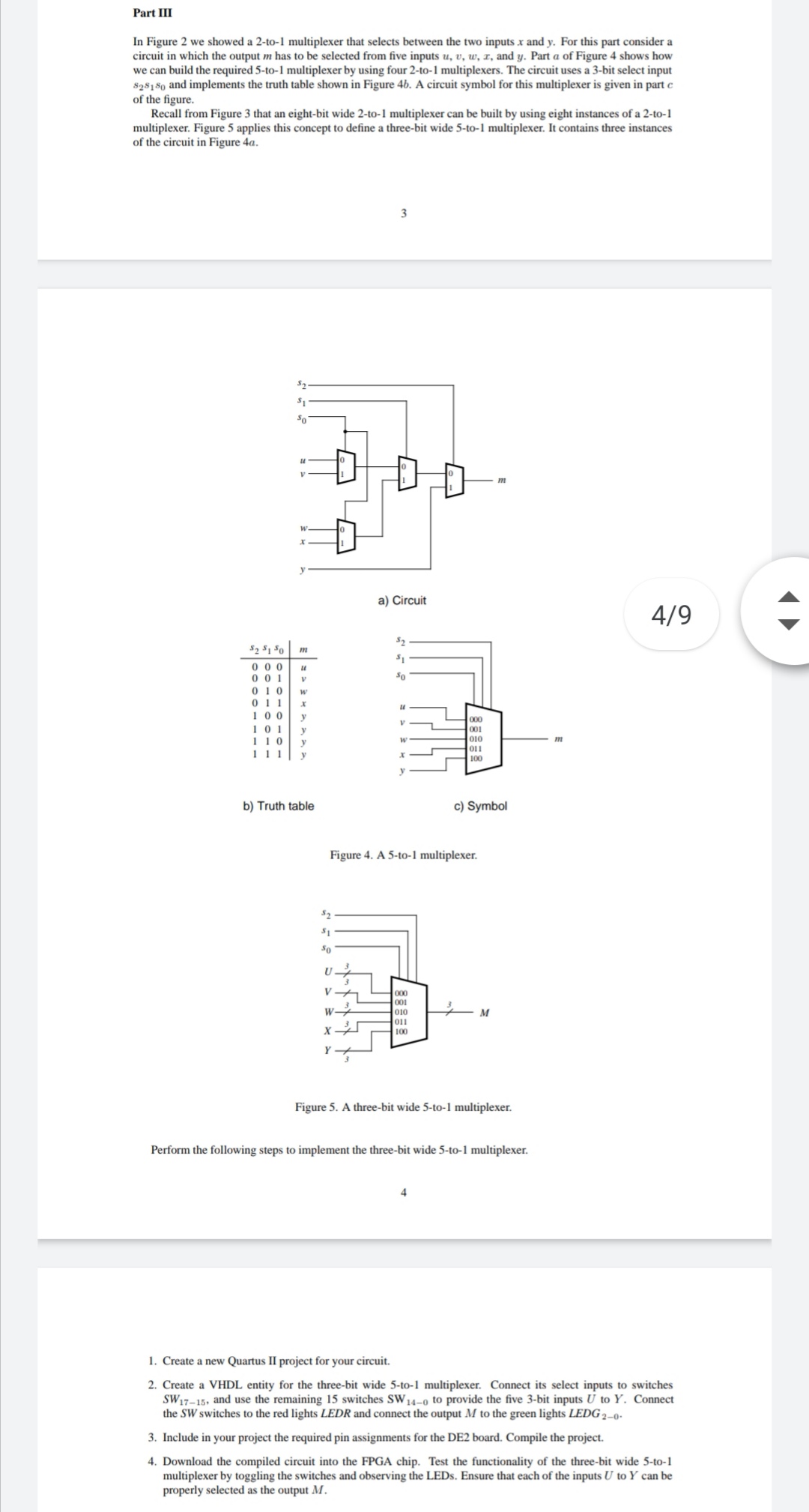
Part III In Figure 2 we showed a 2-to-1 multiplexer that selects between the two inputs x and y. For this part consider a circuit in which the output m has to be selected from five inputs u, v, w, I, and y. Part a of Figure 4 shows how we can build the required 5-to-1 multiplexer by using four 2-to-1 multiplexers. The circuit uses a 3-bit select input 828180 and implements the truth table shown in Figure 46. A circuit symbol for this multiplexer is given in parte of the figure. Recall from Figure 3 that an eight-bit wide 2-to-1 multiplexer can be built by using eight instances of a 2-to-1 multiplexer. Figure 5 applies this concept to define a three-bit wide 5-to-1 multiplexer. It contains three instances of the circuit in Figure 4a. 3 $2 $1 so m a) Circuit 4/9 M $2 $1 50 $2$150 000 u 001 V 010 w 011 100 y 101 y 110 111ly 000 00: 010 OI 100 b) Truth table c) Symbol Figure 4. A 5-to-1 multiplexer. 52 $1 50 u 000 001 010 011 100 M Figure 5. A three-bit wide 5-to-1 multiplexer. Perform the following steps to implement the three-bit wide 5-to-1 multiplexer. 4 1. Create a new Quartus II project for your circuit 2. Create a VHDL entity for the three-bit wide 5-to-1 multiplexer. Connect its select inputs to switches SW17-15, and use the remaining 15 switches SW 14-0 to provide the five 3-bit inputs U to Y. Connect the SW switches to the red lights LEDR and connect the output M to the green lights LEDG 2-0. 3. Include in your project the required pin assignments for the DE2 board. Compile the project. 4. Download the compiled circuit into the FPGA chip. Test the functionality of the three-bit wide 5-to-1 multiplexer by toggling the switches and observing the LEDs. Ensure that each of the inputs U to Y can be properly selected as the output M. Part III In Figure 2 we showed a 2-to-1 multiplexer that selects between the two inputs x and y. For this part consider a circuit in which the output m has to be selected from five inputs u, v, w, I, and y. Part a of Figure 4 shows how we can build the required 5-to-1 multiplexer by using four 2-to-1 multiplexers. The circuit uses a 3-bit select input 828180 and implements the truth table shown in Figure 46. A circuit symbol for this multiplexer is given in parte of the figure. Recall from Figure 3 that an eight-bit wide 2-to-1 multiplexer can be built by using eight instances of a 2-to-1 multiplexer. Figure 5 applies this concept to define a three-bit wide 5-to-1 multiplexer. It contains three instances of the circuit in Figure 4a. 3 $2 $1 so m a) Circuit 4/9 M $2 $1 50 $2$150 000 u 001 V 010 w 011 100 y 101 y 110 111ly 000 00: 010 OI 100 b) Truth table c) Symbol Figure 4. A 5-to-1 multiplexer. 52 $1 50 u 000 001 010 011 100 M Figure 5. A three-bit wide 5-to-1 multiplexer. Perform the following steps to implement the three-bit wide 5-to-1 multiplexer. 4 1. Create a new Quartus II project for your circuit 2. Create a VHDL entity for the three-bit wide 5-to-1 multiplexer. Connect its select inputs to switches SW17-15, and use the remaining 15 switches SW 14-0 to provide the five 3-bit inputs U to Y. Connect the SW switches to the red lights LEDR and connect the output M to the green lights LEDG 2-0. 3. Include in your project the required pin assignments for the DE2 board. Compile the project. 4. Download the compiled circuit into the FPGA chip. Test the functionality of the three-bit wide 5-to-1 multiplexer by toggling the switches and observing the LEDs. Ensure that each of the inputs U to Y can be properly selected as the output M


