

Answered step by step
Verified Expert Solution
Question
1 Approved Answer
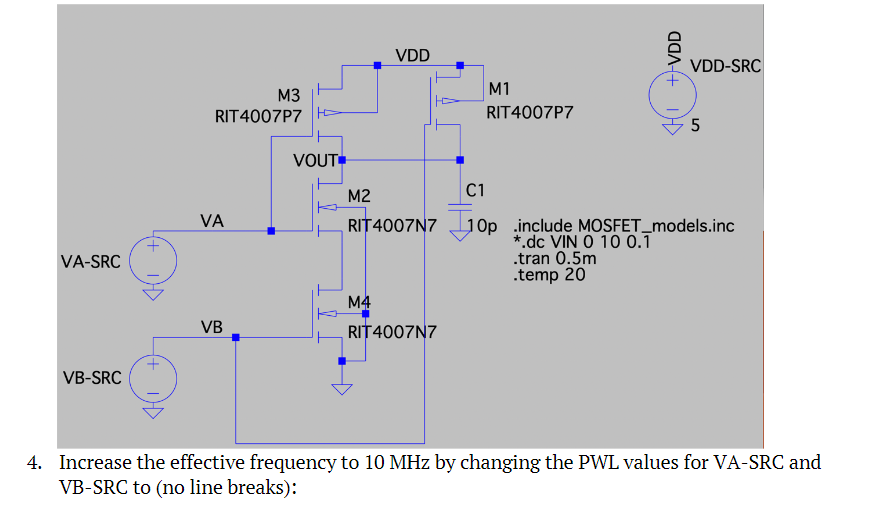
PERFORM THIS IN LTSPICE AND PROVIDE ANSWERS PLEASE GAURANTEED THUMBS UP 1. Let's build a NAND gate. Save your inverter with a new name like
 PERFORM THIS IN LTSPICE AND PROVIDE ANSWERS PLEASE GAURANTEED THUMBS UP
Step by Step Solution
There are 3 Steps involved in it
Step: 1

Get Instant Access to Expert-Tailored Solutions
See step-by-step solutions with expert insights and AI powered tools for academic success
Step: 2

Step: 3
Ace Your Homework with AI
Get the answers you need in no time with our AI-driven, step-by-step assistance
Get Started
Big Data, Mining, And Analytics Components Of Strategic Decision Making
Authors: Stephan Kudyba
1st Edition
1466568704, 9781466568709