Question: Please answer table 18-3 and 18-4, and draw the logic diagram. Thank you. d) Changing the MOD-number of a counter: In the preceding step, you
Please answer table 18-3 and 18-4, and draw the logic diagram. Thank you. 
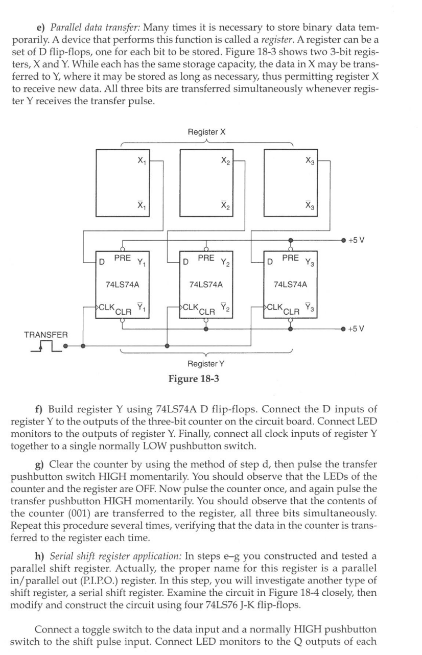
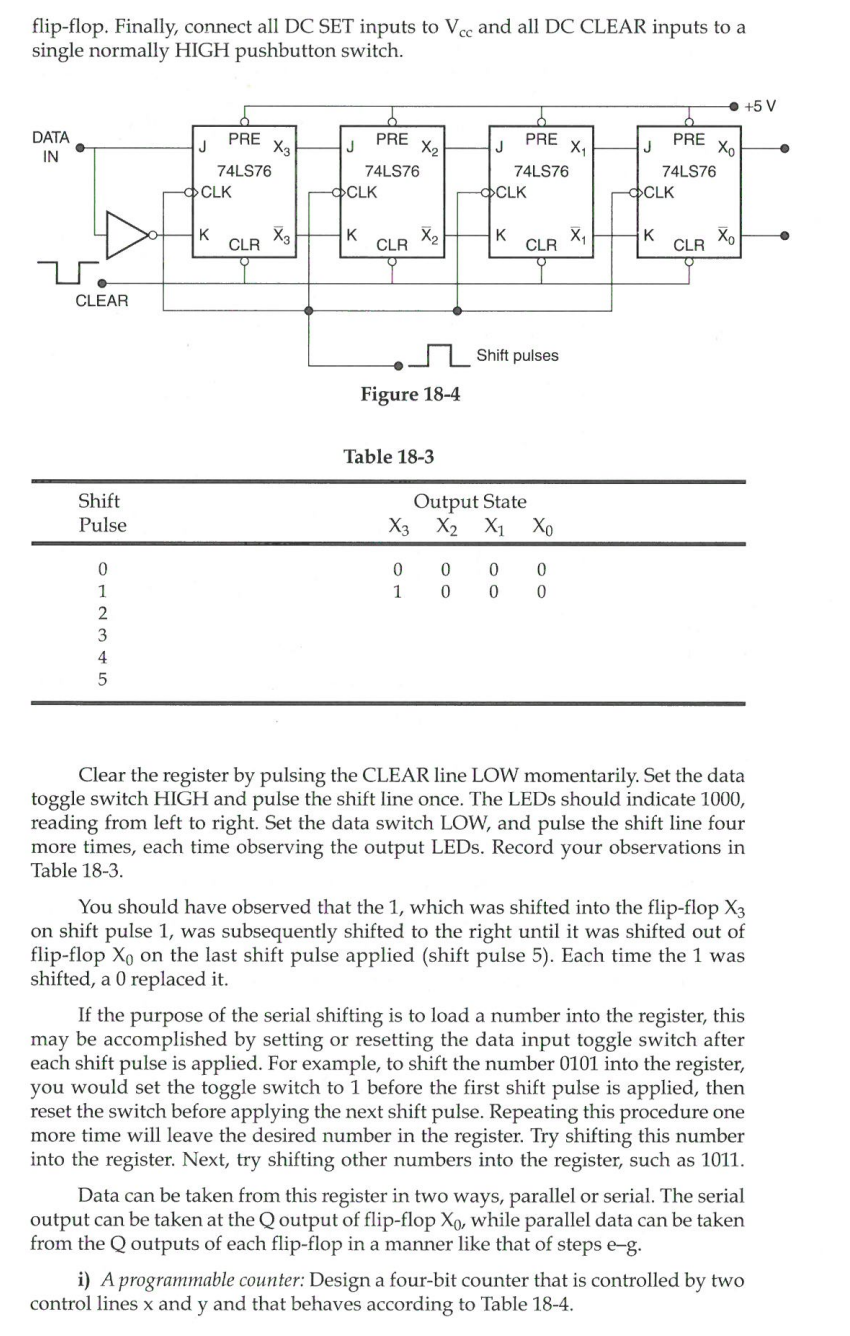
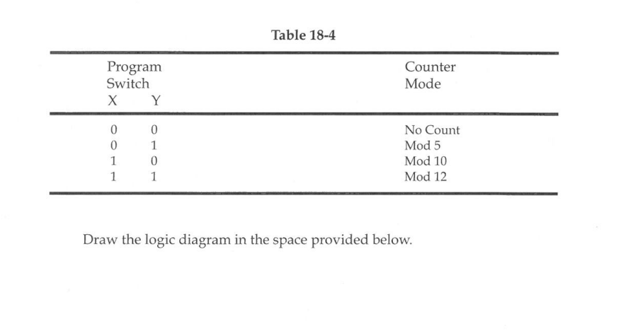
d) Changing the MOD-number of a counter: In the preceding step, you investigated a three-bit counter. You determined its MOD-number and its count sequence. You will now modify the counter so that it has a new count sequence and a new MOD-number. Disconnect the pushbutton switch from the DC CLEAR inputs of the flipflops. Modify the counter circuit so that the wiring is like that shown in Figure 18-2. Clear the counter by pulsing it until the LED monitors indicate a count of 000 , or by lifting the DC CLEAR line connection from the NAND gate output and grounding it momentarily, then reconnecting it to the NAND gate. Using Table 18-2, record the counter output states you observe as you pulse the counter through its new count sequence. Determine the MOD-number of this counter by examining the counter sequence: e) Parallel data transfer: Many times it is necessary to store binary data temporarily. A device that performs this function is called a register. A register can be a set of D flip-flops, one for each bit to be stored. Figure 18-3 shows two 3-bit registers, X and Y. While each has the same storage capacity, the data in X may be transferred to Y, where it may be stored as long as necessary, thus permitting register X to receive new data. All three bits are transferred simultaneously whenever register Y receives the transfer pulse. f) Build register Y using 74LS74A D flip-flops. Connect the D inputs of register Y to the outputs of the three-bit counter on the circuit board. Connect LED monitors to the outputs of register Y. Finally, connect all clock inputs of register Y together to a single normally LOW pushbutton switch. g) Clear the counter by using the method of step d, then pulse the transfer pushbutton switch HIGH momentarily. You should observe that the LEDs of the counter and the register are OFF. Now pulse the counter once, and again pulse the transfer pushbutton HIGH momentarily. You should observe that the contents of the counter (001) are transferred to the register, all three bits simultaneously. Repeat this procedure several times, verifying that the data in the counter is transferred to the register each time. h) Serial shift register application: In steps e-g you constructed and tested a parallel shift register. Actually, the proper name for this register is a parallel in/parallel out (P.I.P.O.) register. In this step, you will investigate another type of shift register, a serial shift register. Examine the circuit in Figure 18-4 closely, then modify and construct the circuit using four 74LS76 J-K flip-flops. Connect a toggle switch to the data input and a normally HIGH pushbutton switch to the shift pulse input. Connect LED monitors to the Q outputs of each flip-flop. Finally, connect all DC SET inputs to Vcc and all DC CLEAR inputs to a single normally HIGH pushbutton switch. Table 18-3 Clear the register by pulsing the CLEAR line LOW momentarily. Set the data toggle switch HIGH and pulse the shift line once. The LEDs should indicate 1000, reading from left to right. Set the data switch LOW, and pulse the shift line four more times, each time observing the output LEDs. Record your observations in Table 18-3. You should have observed that the 1 , which was shifted into the flip-flop X3 on shift pulse 1 , was subsequently shifted to the right until it was shifted out of flip-flop X0 on the last shift pulse applied (shift pulse 5). Each time the 1 was shifted, a 0 replaced it. If the purpose of the serial shifting is to load a number into the register, this may be accomplished by setting or resetting the data input toggle switch after each shift pulse is applied. For example, to shift the number 0101 into the register, you would set the toggle switch to 1 before the first shift pulse is applied, then reset the switch before applying the next shift pulse. Repeating this procedure one more time will leave the desired number in the register. Try shifting this number into the register. Next, try shifting other numbers into the register, such as 1011. Data can be taken from this register in two ways, parallel or serial. The serial output can be taken at the Q output of flip-flop X0, while parallel data can be taken from the Q outputs of each flip-flop in a manner like that of steps e-g. i) A programmable counter: Design a four-bit counter that is controlled by two control lines x and y and that behaves according to Table 18-4. Draw the logic diagram in the space provided below. d) Changing the MOD-number of a counter: In the preceding step, you investigated a three-bit counter. You determined its MOD-number and its count sequence. You will now modify the counter so that it has a new count sequence and a new MOD-number. Disconnect the pushbutton switch from the DC CLEAR inputs of the flipflops. Modify the counter circuit so that the wiring is like that shown in Figure 18-2. Clear the counter by pulsing it until the LED monitors indicate a count of 000 , or by lifting the DC CLEAR line connection from the NAND gate output and grounding it momentarily, then reconnecting it to the NAND gate. Using Table 18-2, record the counter output states you observe as you pulse the counter through its new count sequence. Determine the MOD-number of this counter by examining the counter sequence: e) Parallel data transfer: Many times it is necessary to store binary data temporarily. A device that performs this function is called a register. A register can be a set of D flip-flops, one for each bit to be stored. Figure 18-3 shows two 3-bit registers, X and Y. While each has the same storage capacity, the data in X may be transferred to Y, where it may be stored as long as necessary, thus permitting register X to receive new data. All three bits are transferred simultaneously whenever register Y receives the transfer pulse. f) Build register Y using 74LS74A D flip-flops. Connect the D inputs of register Y to the outputs of the three-bit counter on the circuit board. Connect LED monitors to the outputs of register Y. Finally, connect all clock inputs of register Y together to a single normally LOW pushbutton switch. g) Clear the counter by using the method of step d, then pulse the transfer pushbutton switch HIGH momentarily. You should observe that the LEDs of the counter and the register are OFF. Now pulse the counter once, and again pulse the transfer pushbutton HIGH momentarily. You should observe that the contents of the counter (001) are transferred to the register, all three bits simultaneously. Repeat this procedure several times, verifying that the data in the counter is transferred to the register each time. h) Serial shift register application: In steps e-g you constructed and tested a parallel shift register. Actually, the proper name for this register is a parallel in/parallel out (P.I.P.O.) register. In this step, you will investigate another type of shift register, a serial shift register. Examine the circuit in Figure 18-4 closely, then modify and construct the circuit using four 74LS76 J-K flip-flops. Connect a toggle switch to the data input and a normally HIGH pushbutton switch to the shift pulse input. Connect LED monitors to the Q outputs of each flip-flop. Finally, connect all DC SET inputs to Vcc and all DC CLEAR inputs to a single normally HIGH pushbutton switch. Table 18-3 Clear the register by pulsing the CLEAR line LOW momentarily. Set the data toggle switch HIGH and pulse the shift line once. The LEDs should indicate 1000, reading from left to right. Set the data switch LOW, and pulse the shift line four more times, each time observing the output LEDs. Record your observations in Table 18-3. You should have observed that the 1 , which was shifted into the flip-flop X3 on shift pulse 1 , was subsequently shifted to the right until it was shifted out of flip-flop X0 on the last shift pulse applied (shift pulse 5). Each time the 1 was shifted, a 0 replaced it. If the purpose of the serial shifting is to load a number into the register, this may be accomplished by setting or resetting the data input toggle switch after each shift pulse is applied. For example, to shift the number 0101 into the register, you would set the toggle switch to 1 before the first shift pulse is applied, then reset the switch before applying the next shift pulse. Repeating this procedure one more time will leave the desired number in the register. Try shifting this number into the register. Next, try shifting other numbers into the register, such as 1011. Data can be taken from this register in two ways, parallel or serial. The serial output can be taken at the Q output of flip-flop X0, while parallel data can be taken from the Q outputs of each flip-flop in a manner like that of steps e-g. i) A programmable counter: Design a four-bit counter that is controlled by two control lines x and y and that behaves according to Table 18-4. Draw the logic diagram in the space provided below
Step by Step Solution
There are 3 Steps involved in it

Get step-by-step solutions from verified subject matter experts


