Answered step by step
Verified Expert Solution
Question
1 Approved Answer
Please Complete and Explain. Thank You! 1 The Objective The principle objective of this part is to have you gain familiarity with several gate level


Please Complete and Explain. Thank You!
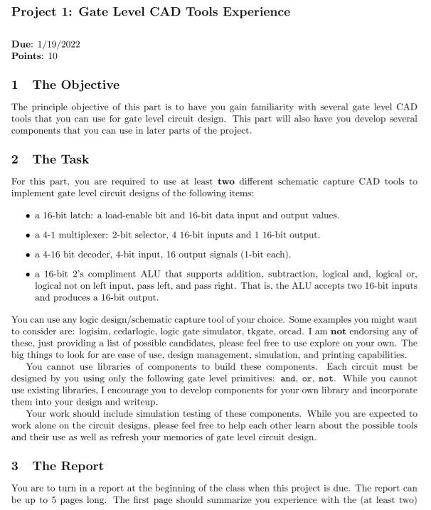
1 The Objective The principle objective of this part is to have you gain familiarity with several gate level CAD tools that you can use for gate level circuit design. This part will also have you develop several components that you can use in later parts of the project. 2 The Task For this part, you are required to use at least two different schematic capture CAD tools to implement gate level circuit designs of the following items: - a 16-bit latch: a load-enable bit and 16-bit data input and output values. - a 4-1 multiplexer: 2-bit selector, 4 16-bit inputs and 1 16-bit output. - a 4-16 bit decoder, 4-bit input, 16 output signals (1-bit each). - a 16-bit 2's compliment ALU that supports addition, subtraction, logical and, logical or, logical not on left input, pass left, and pass right. That is, the ALU accepts two 16-bit inputs and produces a 16-bit output. You can use any logic design/schematic capture tool of your choice. Some examples you might want to consider are: logisim, cedarlogic, logic gate simulator, tkgate, orcad. I am not endorsing any of these, just providing a list of possible candidates, please feel free to use explore on your own. The big things to look for are ease of use, design management, simulation, and printing capabilities. You cannot use libraries of components to build these components. Each circuit must be designed by you using only the following gate level primitives: and, or, not. While you cannot use existing libraries, I encourage you to develop components for your own library and incorporate them into your design and writeup. Your work should include simulation testing of these components. While you are expected to work alone on the circuit designs, please feel free to help each other learn about the possible tools and their use as well as refresh your memories of gate level circuit design. 3 The Report You are to turn in a report at the beginning of the class when this project is due. The report can be up to 5 pages long. The first page should summarize you experience with the (at least two) different CAD tools that you used to design these circuits. This page should include a discussion of the pros and cons of each tool. Each of the remaining 4 pages should document each of the four circuits you designed for this part - one page per circuit and one circuit per page (you do not need to show the circuit solutions from both CAD tools). This part should be mostly a review of your digital logic class. The real challenge with this part is the communication of a reasonably complex circuit in a single page - find a modular presentation style. Perhaps a bit slice through the circuit formed into a block and then a block diagram. Displaying the entire circuit in one image is not an acceptable solutionStep by Step Solution
There are 3 Steps involved in it
Step: 1

Get Instant Access to Expert-Tailored Solutions
See step-by-step solutions with expert insights and AI powered tools for academic success
Step: 2

Step: 3

Ace Your Homework with AI
Get the answers you need in no time with our AI-driven, step-by-step assistance
Get Started


