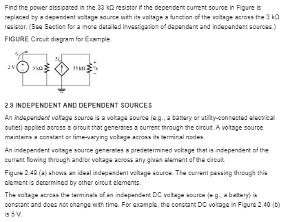


please help me:-
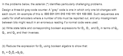
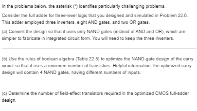
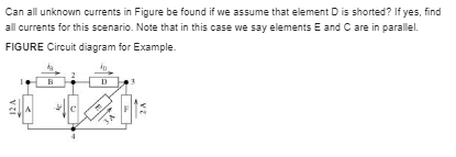
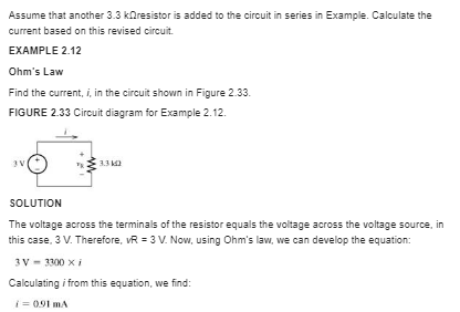
B refers to Basic, A refers to Average, H refers to Hard, and * refers to problems with answers. (A) Find the number of electrons, n, as a function of time if:B refers to Basic, A refers to Average, H refers to Hard, and * refers to problems with answers. (A)* Direct current in steady state does not vary with time. If a DC currentof 5 A flows through a wire, find the charge through the wire with respect to time. The charge at = 0 is 0.B refers to Basic, A refers to Average, H refers to Hard, and * refers to problems with answers. (H) Application: electroplating A depth of 0.15 mm nickel is required to be coated on a metal surface by electroplating. The nickel density p = 8.8 x 10³ kg/m3. the electrochemical equivalent (= 0.304 x 10⁻⁶ kg/C (which is the weight of the nickel produced by electrolysis during the flow of a quantity of electricity equal to 1 (), and the current per square meter p = 35 A/m2. How long does it take to achieve the desired coating depth? (Hint: Find the mass of the nickel.)In the problems below, the asterisk (") identifies particularly challenging problems. Design a three-bit gray-code counter. A "gray" code is one in which only one bit changes with each count. An example of this is: 000 001 011 010 110 111 101 100 000. Such sequences are useful for shaft encoders where a number of bits must be reported out, and any misalignment between bits might result in an erroneous reading if a normal code were used. (3) Write state table and corresponding boolean expressions for D., D,, and D, in terms of Q,. Qy, and Q, and their inverses. (b) Reduce the expression for Do using boolean algebra to show that: +Q.QIn the problems below, the asterisk (") identifies particularly challenging problems. Draw the schematic for the gray-code state machine, given that D, = Q,90+Q2 Q,QJ You may use LogicWorks" or a similar program to produce a neat schematic and to allow you to verify its operation.Describe concisely in your own words the computer terms represented by each of the following acronyms: BIOS. MPEG, JPEG. CISC, RISC, modem, USB.Can all unknown currents in Figure be found if we assume that element D is shorted? If yes, find all currents for this scenario. Note that in this case we say elements E and C are in parallel. FIGURE Circuit diagram for Example. In 12 4B refers to Basic, A refers to Average, H refers to Hard, and * refers to problems with answers. (B) Identify the device in Figure: FIGURE Image for Problem.Assume that another 3.3 koresistor is added to the circuit in series in Example. Calculate the current based on this revised circuit. EXAMPLE 2.12 Ohm's Law Find the current, i, in the circuit shown in Figure 2 33. FIGURE 2.33 Circuit diagram for Example 2.12. THEE SOLUTION The voltage across the terminals of the resistor equals the voltage across the voltage source, in this case. 3 V. Therefore, vR = 3 V. Now, using Ohm's law, we can develop the equation: Calculating i from this equation, we find: 1= 091 A\fIn the problems below, the asterisk (") identifies particularly challenging problems. Convert the three following base-10 numbers to binary numbers: 5, 87, and 20.125.In the problems below, the asterisk (") identifies particularly challenging problems. Find the sums of the following pairs of binary numbers, and check your answers in the base-10 system: (3) 01111 and 00001 (b) 10001 and 01010In the problems below, the asterisk (") identifies particularly challenging problems. Multiply the following binary numbers, and check your answers in the base-10 system: (=) 10101 and 00001 (b) 10101 and 00010 (c) 11111 and 00101In this problem below, the asterisk ("] identifies particularly challenging problems. Using a program such as LogicWorks , simulain a synchronous counter, made of interconnected gates and flip-flops, that will count from 0 to 15 clock pulses.In the problems below, the asterisk (") identifies particularly challenging problems. Consider the full adder for three-level logic that you designed and simulated in Problem 22.8. This adder employed three inverters, eight AND gates, and two OR gates. (3) Convert the design so that it uses only NAND gates (instead of AND and OR), which are simpler to fabricate in integrated circuit form. You will need to keep the three inverters. (b) Use the rules of boolean algebra (Table 22 5) to optimize the NAND-gate design of the carry circuit so that it uses a minimum number of transistors. Helpful information: the optimized carry design will contain 4 NAND gates. having different numbers of inputs. (c) Determine the number of field-effect transistors required in the optimized CMOS full-adder design.In the problems below, the asterisk (") identifies particularly challenging problems. Multiplier. Given a full adder (FA) block (Figure 22 3), design a multiplier to multiply & bits by 8 bits, yielding a 16-bit product using FAs and AND gates


