Answered step by step
Verified Expert Solution
Question
1 Approved Answer
please, include the assembly program too. thank you MSP430 Assembly Programming Intermediate Memory Map, Assembly Directives, and Comparisons In this lab, you will be designing
please, include the assembly program too. thank you
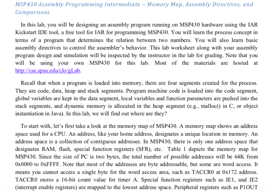
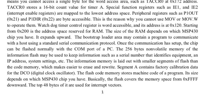
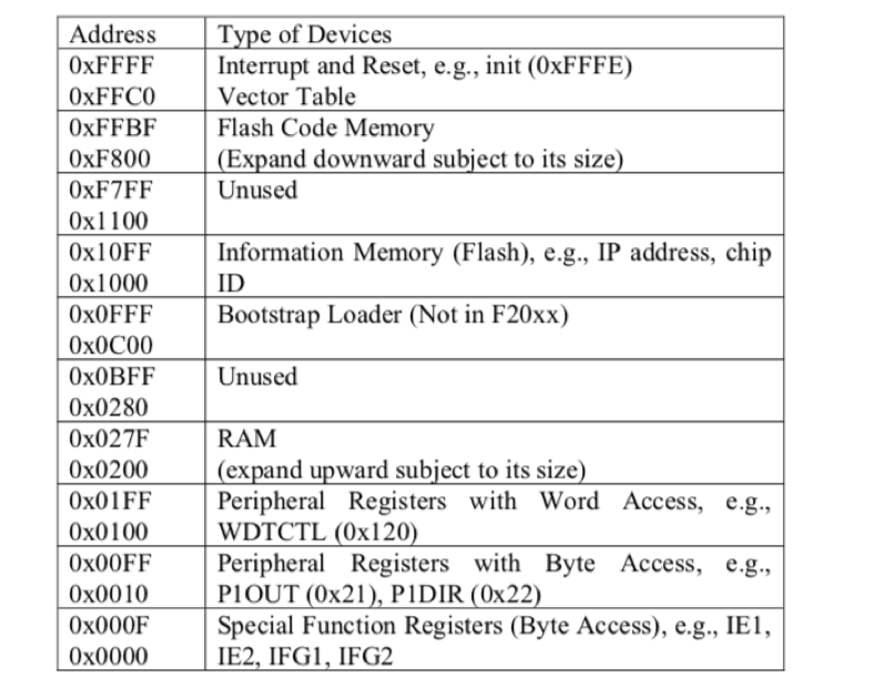
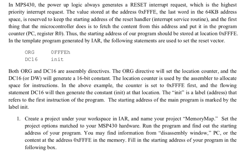
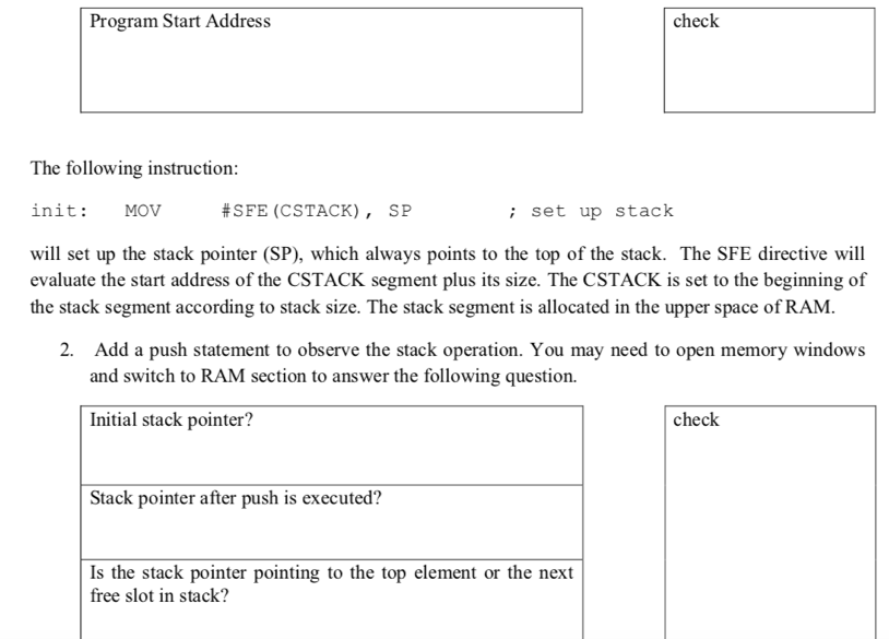
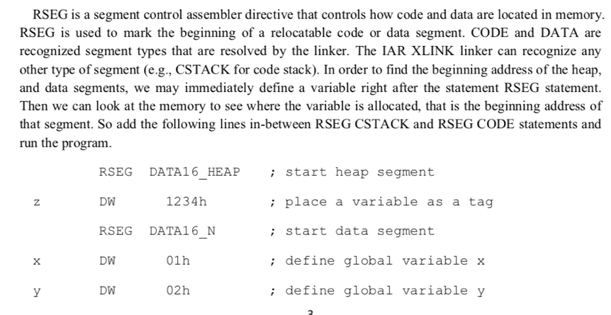
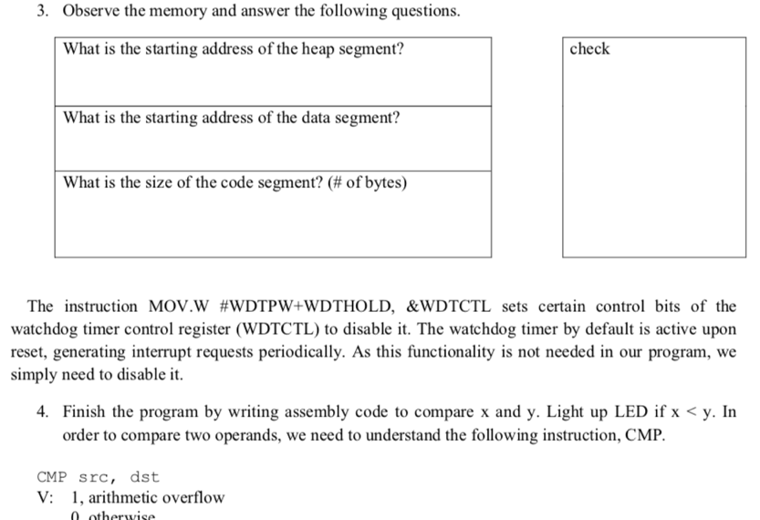
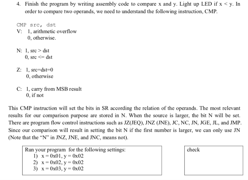
MSP430 Assembly Programming Intermediate Memory Map, Assembly Directives, and Comparisons In this lab, you will be designing an assembly program running on MSP430 hardware using the IAR Kickstart IDE tool, a free tool for IAR for programming MSP430. You will learn the process concept in terms of a program that determines the relation between two numbers. You will also learn basic assembly directives to control the assembler's behavior. This lab worksheet along with your assembl:y program design and simulation will be inspected by the instructor in the lab for grading. Note that you will be using your own MSP430 for this lab. Most of the materials are hosted at http://cse.spsu.edu/clo/gLab Recall that when a program is loaded into memory, there are four segments created for the process They are code, data, heap and stack segments. Program machine code is loaded into the code segment, global variables are kept in the data segment, local variables and function parameters are pushed into the stack segments, and dynamic memory is allocated in the heap segment (e.g., malloc) in C, or objeot instantiation in Java). In this lab, we will find out where are they? To start with, let's first take a look at the memory map of MSP430. A memory map shows an address space used for a CPU. An address, like your home address, designates a unique location in memory. An address space is a collection of contiguous addresses. In MSP430, there is only one address space that designates RAM, flash, special function registers (SFR), etc. Table 1 depicts the memory map for MSP430. Since the size of PC is two bytes, the total number of possible addresses will be 64K from 0x0000 to 0xFFFF. Note that most of the addresses are byte addressable, but some are word access. It means you cannot access a single byte for the word access area, such as TACCRO at 0x172 address TACCRO stores a 16-bit count value for timer A. Special function registers such as IE and IE2 (interrupt enable registers) are mapped to the lowest address space. Peripheral registers such as PIOUT means you cannot access a single byte for the word access area, such as TACCRO at 0xl72 address. TACCRO stores a 16-bit count value for timer A. Special function registers such as IEl, and IE2 (interrupt enable registers) are mapped to the lowest address space. Peripheral registers such as PIOUT (0x21) and PIDIR (0x22) are byte accessible. This is the reason why you cannot use MOV or MOV.W to operate them. Watch dog timer control register is word accessible, and its address is at 0x 120. Starting from 0x200 is the address space reserved for RAM. The size of the RAM depends on which MSP430 chip you have. It expands upward. The bootstrap loader area may contain a program to communicate with a host using a standard serial communication protocol. Once the communication has setup, the chip can be flashed normally with the COM port of a PC. The 256 bytes nonvolatile memory of the information flash may be used to keep information such as a serial number that identifies equipment, an IP address, system settings, etc. The information memory is laid out with smaller segments of flash than the code memory, which makes easier to erase and rewrite. Segment A contains factory calibration data for the DCO (digital clock oscillator). The flash code memory stores machine code of a program. Its size depends on which MSP430 chip you have. Basically, the flash covers the memory space from 0xFFFF downward. The top 48 bytes of it are used for interrupt vectors 1 Address Type of Devices 0xFFFF Interrupt and Reset, e.g., init (OxFFFE) 0xFFCO 0xFFBF 0xF800 0xF7FF 0x1100 0x10FF Information Memory (Flash), e.g., IP address, chip 0x1000 0xOFFF Bootstrap Loader (Not in F20xx) 0x0C00 OxOBFF 0x0280 0x027F 0x0200 0x01FF 0x0100 Ox00FF 0x0010 0x000F Special Function Registers (Byte Access), e.g., IE1, 0x0000 Vector Table Flash Code Memory Expand downward subject to its size Unused ID Unused RAM expand upward subject to its size Peripheral Registers with Word Access, e.g WDTCTL (0x120 Peripheral Registers with Byte Access, e.g., PlOUT (0x2), P1DIR (0x22 IE2, IFG1, IFG2 In MPS430, the power up logic always generates a RESET interrupt request, which is the highest priority interrupt request. The value stored at the address OxFFFE, the last word in the 64KB address space, is reserved to keep the starting address of the reset handler (interrupt service routine), and the first thing that the microcontroller does is to fetch the content from this address and put it in the program counter (PC, register RO). Thus, the starting address of our program should be stored at location OxFFFE In the template program generated by IAR, the following statements are used to set the reset vector. ORG DC16 OFFFEh init Both ORG and DC16 are assembly directives. The ORG directive will set the location counter, and the DC16 (or DW) will generate a 16-bit constant. The location counter is used by the assembler to allocate space for instructions. In the above example, the counter is set to 0xFFFE first, and the flowing statement DC16 will then generate the constant (init) at that location. The "init" is a label (address) that refers to the first instruction of the program. The starting address of the main program is marked by the abel ini Create a project under your workspace in IAR, and name your project "MemoryMap." Set the project options matched to your MSP430 hardware. Run the program and find out the starting address of your program. You may find information from "disassembly window," PC, or the content at the address 0xFFFE in the memory. Fil in the starting address of your program in the following box. Program Start Address check The following instruction init: MOV #SFE (CSTACK), SP : set up stack will set up the stack pointer (SP), which always points to the top of the stack. The SFE directive will evaluate the start address of the CSTACK segment plus its size. The CSTACK is set to the beginning of the stack segment according to stack size. The stack segment is allocated in the upper space of RAM. 2. Add a push statement to observe the stack operation. You may need to open memory windows and switch to RAM section to answer the following question. Initial stack pointer? check Stack pointer after push is executed? Is the stack pointer pointing to the top element or the next free slot in stack? RSEG is a segment control assembler directive that controls how code and data are located in memory. RSEG is used to mark the beginning of a relocatable code or data segment. CODE and DATA are recognized segment types that are resolved by the linker. The IAR XLINK linker can recognize any other type of segment (e.g., CSTACK for code stack). In order to find the beginning address of the heap, and data segments, we may immediately define a variable right after the statement RSEG statement. Then we can look at the memory to see where the variable is allocated, that is the beginning address of that segment. So add the following lines in-between RSEG CSTACK and RSEG CODE statements and run the program RSEG DATA16_HEAP start heap segment DW 1234h ;place a variable as a tag ; start data segment ; define global variable x ; define global variabley Z. RSEG DATA16_N DW DW 01h 02h 3. Observe the memory and answer the following questions. What is the starting address of the heap segment? check What is the starting address of the data segment? What is the size of the code segment? (# of bytes) The instruction MOV.W #WDTPW+WDTHOLD, &WDTCTL sets certain control bits of the watchdog timer control register (WDTCTL) to disable it. The watchdog timer by default is active upon reset, generating interrupt requests periodically. As this functionality is not needed in our program, we simply need to disable it 4 Finish the program by writing assembly code to compare x and y. Light up LED if xStep by Step Solution
There are 3 Steps involved in it
Step: 1

Get Instant Access to Expert-Tailored Solutions
See step-by-step solutions with expert insights and AI powered tools for academic success
Step: 2

Step: 3

Ace Your Homework with AI
Get the answers you need in no time with our AI-driven, step-by-step assistance
Get Started


