Question
Please Provide a Matlab Code for it! Thank you in advance! A)This study will look at carrier statistics in intrinsic and extrinsic semiconductors. Use a
Please Provide a Matlab Code for it! Thank you in advance!
A)This study will look at carrier statistics in intrinsic and extrinsic semiconductors. Use a computer to generate plots of the parameters requested below.
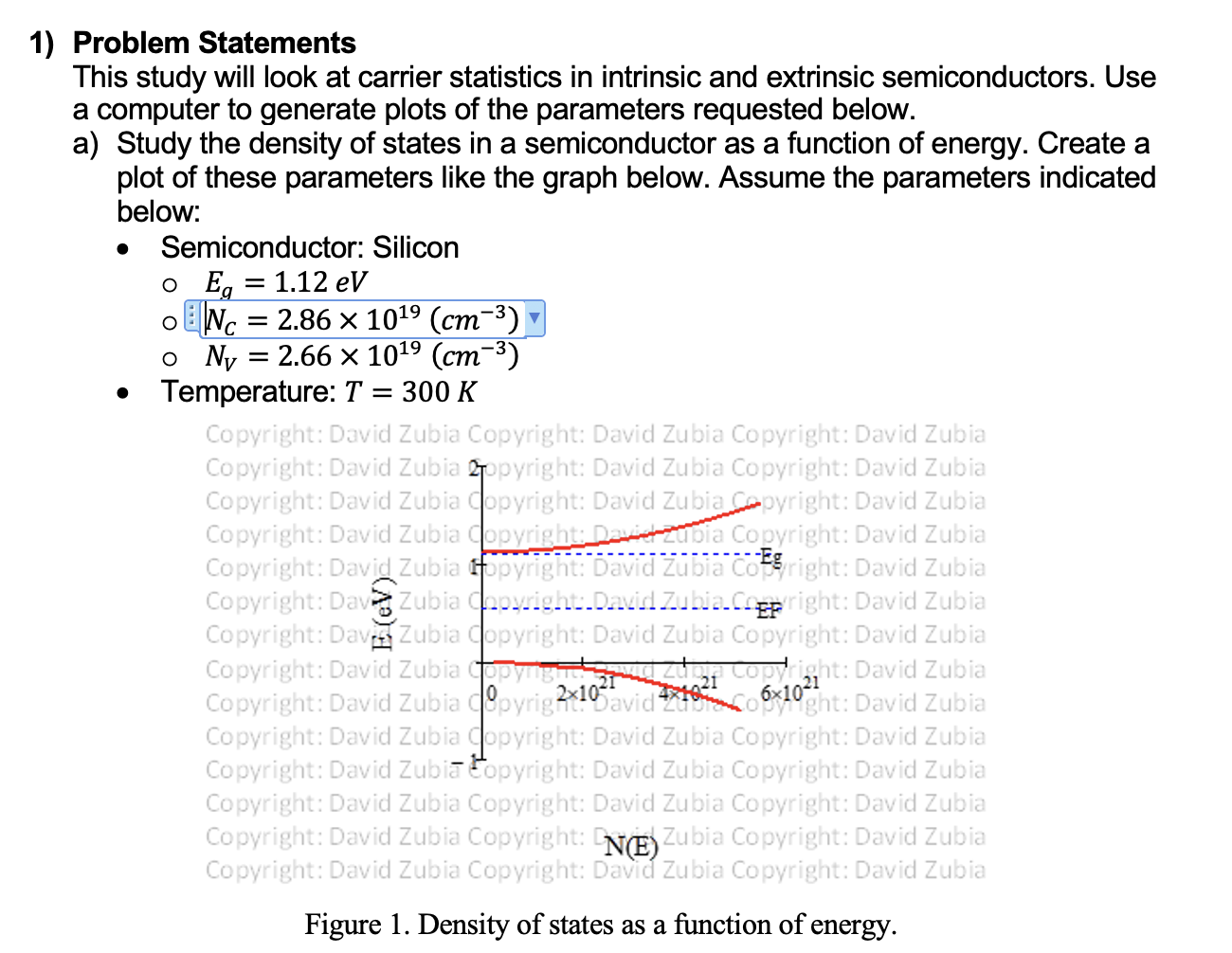
Study the density of states in a semiconductor as a function of energy. Create a plot of these parameters like the graph below. Assume the parameters indicated below:
Semiconductor: Silicon
Eg=1.12eV
Nc=2.86X10¹⁹(cm-3)
Nv=2.66X10¹⁹(cm-3)
Temperature: 300K
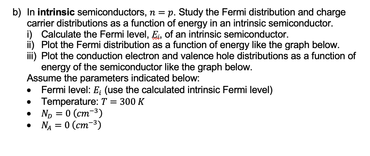
B)In intrinsic semiconductors, n=p. Study the Fermi distribution and charge carrier distributions as a function of energy in an intrinsic semiconductor.
Calculate the Fermi level, Ei, of an intrinsic semiconductor.
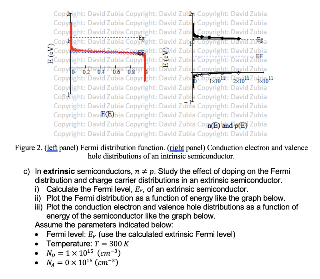
Plot the Fermi distribution as a function of energy like the graph below.
Plot the conduction electron and valence hole distributions as a function of energy of the semiconductor like the graph below.
Assume the parameters indicated below:
Fermi level: Ei (use the calculated intrinsic Fermi level)
Temperature: 300K
ND=0(cm-3)
NA=0(cm-3)
C) In extrinsic semiconductors, n not equal to p. Study the effect of doping on the Fermi distribution and charge carrier distributions in an extrinsic semiconductor.
Calculate the Fermi level, EF, of an extrinsic semiconductor.
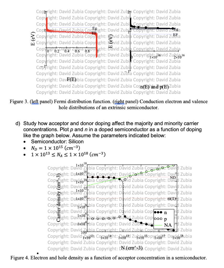
Plot the Fermi distribution as a function of energy like the graph below.
Plot the conduction electron and valence hole distributions as a function of energy of the semiconductor like the graph below.
Assume the parameters indicated below:
Fermi level: EF (use the calculated extrinsic Fermi level)
Temperature: 300K
ND=1X10¹⁵(cm-3)
NA=0X1015(cm-3)
D) Study how acceptor and donor doping affect the majority and minority carrier concentrations. Plot p and n in a doped semiconductor as a function of doping like the graph below. Assume the parameters indicated below:
Semiconductor: Silicon
ND= 1X10¹⁵(cm-3)
1X10¹³ NA
NA 1X1818(cm-3)


Problem Statements This study will look at carrier statistics in intrinsic and extrinsic semiconductors. Use a computer to generate plots of the parameters requested below. a) Study the density of states in a semiconductor as a function of energy. Create a plot of these parameters like the graph below. Assume the parameters indicated below: - Semiconductor: Silicon - Eg=1.12eV o [NC=2.861019(cm3) NV=2.661019(cm3) - Temperature: T=300K Copyright: David Zubia Copyright: David Zubia Copyright: David Zubia Copyright: David Zubia 2 appright: David Zubia Copyright: David Zubia Copyright: David Zubia Oopyright: David Zubia-poprepright: David Zubia Copyright: David Zubia afpyright: David Zbia Co-Eg right: David Zubia Copyright: Davery Zubia Copyright: David Zubia Copyright: David Zubia Copyright: David Zubia Copyright: David Zubia Sopyright: David Zubia Copyright: David Zubia Copyright: David Zubia Copyright: David Zubia Copyright: David Zubia Copyright: David Zubia Copyright: N(E)Z Zubia Copyright: David Zubia Copyright: David Zubia Copyright: David Zubia Copyright: David Zubia Figure 1. Density of states as a function of energy. b) In intrinsic semiconductors, n=p. Study the Fermi distribution and charge carrier distributions as a function of energy in an intrinsic semiconductor. i) Calculate the Fermi level, Ei, of an intrinsic semiconductor. ii) Plot the Fermi distribution as a function of energy like the graph below. iii) Plot the conduction electron and valence hole distributions as a function of energy of the semiconductor like the graph below. Assume the parameters indicated below: - Fermi level: Ei (use the calculated intrinsic Fermi level) - Temperature: T=300K - ND=0(cm3) - NA=0(cm3) Copyright: David Zubia Copyright: David Zla Copyright: David Zubia Copyright: DavF(E) bia Copyright: David Zubia Copyright: David Zubia Copyright: David Zubia Copyright: David Zubia Conn(E) and p(E) Zubia Copyright: David Zubia Copyright: David Zubia Copyright: David Zubia Figure 2. (left panel) Fermi distribution function. (right panel) Conduction electron and valence hole distributions of an intrinsic semiconductor. c) In extrinsic semiconductors, n=p. Study the effect of doping on the Fermi distribution and charge carrier distributions in an extrinsic semiconductor. i) Calculate the Fermi level, EF, of an extrinsic semiconductor. ii) Plot the Fermi distribution as a function of energy like the graph below. iii) Plot the conduction electron and valence hole distributions as a function of energy of the semiconductor like the graph below. Assume the parameters indicated below: - Fermi level: EF (use the calculated extrinsic Fermi level) - Temperature: T=300K - ND=11015(cm3) - NA=01015(cm3) Figure 3. (left panel) Fermi distribution function. (right panel) Conduction electron and valence hole distributions of an extrinsic semiconductor. d) Study how acceptor and donor doping affect the majority and minority carrier concentrations. Plot p and n in a doped semiconductor as a function of doping like the graph below. Assume the parameters indicated below: - Semiconductor: Silicon - ND=11015(cm3) - 11013NA11018(cm3) Figure 4. Electron and hole density as a function of acceptor concentration in a semiconductor
Step by Step Solution
There are 3 Steps involved in it
Step: 1

Get Instant Access to Expert-Tailored Solutions
See step-by-step solutions with expert insights and AI powered tools for academic success
Step: 2

Step: 3

Ace Your Homework with AI
Get the answers you need in no time with our AI-driven, step-by-step assistance
Get Started


