 please provide vhdl coded with simulation
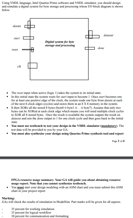
Using VHDL language, Intel Quartus Prime software and VHDL simulator, you should design and simulate a digital system for byte storage and processing whose 1/0 block diagram is shown below datain dataout starr Digital system for byte storage and processing done reset clk The reset input when active (logic 1) takes the system to its initial state. In this initial state the system waits for start input to become 1. Once start becomes one for at least one positive edge of the clock, the system reads one byte from datain at each of the next 8 clock edges (cycles) and stores them in an 8 X 8 memory in the system, It then XORs all the stored 8 bytes (byte bytel e... byte 7). Assume that only two bytes can be XORed at each clock edge which means you will need multiple clock cycles to XOR all 8 stored bytes. Once the result is available the system outputs the result on dataout and sets the done output to 1 for one clock cycle and then goes back to the initial state You must use testbench to test your design in the VHDL simulator (mandatory). The test data will be provided to you by your GA. You must also synthesize your design using Quartus Prime synthesis tool and report Page 1 of 4 FPGA resource usage summary Your GA will guide you about obtaining resource usage report. Note that you cannot synthesize testbench. You must start your design modeling with an ASM chart and you must submit this ASM chart in your project report Marking: GAs will check the results of simulation in ModelSim. Part marks will be given for all aspects. 35 percent for working simulation 35 percent for logical workflow 30 percent for communication and formatting Using VHDL language, Intel Quartus Prime software and VHDL simulator, you should design and simulate a digital system for byte storage and processing whose 1/0 block diagram is shown below datain dataout starr Digital system for byte storage and processing done reset clk The reset input when active (logic 1) takes the system to its initial state. In this initial state the system waits for start input to become 1. Once start becomes one for at least one positive edge of the clock, the system reads one byte from datain at each of the next 8 clock edges (cycles) and stores them in an 8 X 8 memory in the system, It then XORs all the stored 8 bytes (byte bytel e... byte 7). Assume that only two bytes can be XORed at each clock edge which means you will need multiple clock cycles to XOR all 8 stored bytes. Once the result is available the system outputs the result on dataout and sets the done output to 1 for one clock cycle and then goes back to the initial state You must use testbench to test your design in the VHDL simulator (mandatory). The test data will be provided to you by your GA. You must also synthesize your design using Quartus Prime synthesis tool and report Page 1 of 4 FPGA resource usage summary Your GA will guide you about obtaining resource usage report. Note that you cannot synthesize testbench. You must start your design modeling with an ASM chart and you must submit this ASM chart in your project report Marking: GAs will check the results of simulation in ModelSim. Part marks will be given for all aspects. 35 percent for working simulation 35 percent for logical workflow 30 percent for communication and formatting
 please provide vhdl coded with simulation


