Please show design ( truth tables, k-maps, and logic equations).

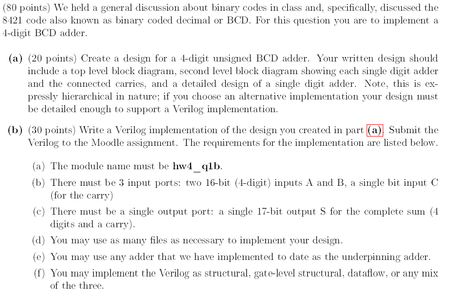
(80 points) We held a general discussion about binary codes in class and, specifically, discussed the 8421 code also known as binary coded decimal or BCD. For this question you are to implement a 4-digit BCD adder. (a) (20 points) Create a design for a 4-digit unsigned BCD adder. Your written design should include a top level block diagram, second level block diagram showing each single digit adder and the connected carries, and a detailed design of a single digit adder. Note, this is ex- pressly hierarchical in nature; if you choose an alternative implementation your design must be detailed enough to support a Verilog implementation. (b) (30 points) Write a Verilog implementation of the design you created in part (a) Submit the Verilog to the Moodle assignment. The requirements for the implementation are listed below. (a) The module name must be hw4_qlb. (b) There must be 3 input ports: two 16-bit (4-digit) inputs A and B, a single bit input C (for the carry) (C) There must be a single output port: a single 17-bit output S for the complete sum (4 digits and a carry). (d) You may use as many files as necessary to implement your design. (e) You may use any adder that we have implemented to date as the underpinning adder. (f) You may implement the Verilog as structural, gate-level structural, dataflow, or any mix of the three. (80 points) We held a general discussion about binary codes in class and, specifically, discussed the 8421 code also known as binary coded decimal or BCD. For this question you are to implement a 4-digit BCD adder. (a) (20 points) Create a design for a 4-digit unsigned BCD adder. Your written design should include a top level block diagram, second level block diagram showing each single digit adder and the connected carries, and a detailed design of a single digit adder. Note, this is ex- pressly hierarchical in nature; if you choose an alternative implementation your design must be detailed enough to support a Verilog implementation. (b) (30 points) Write a Verilog implementation of the design you created in part (a) Submit the Verilog to the Moodle assignment. The requirements for the implementation are listed below. (a) The module name must be hw4_qlb. (b) There must be 3 input ports: two 16-bit (4-digit) inputs A and B, a single bit input C (for the carry) (C) There must be a single output port: a single 17-bit output S for the complete sum (4 digits and a carry). (d) You may use as many files as necessary to implement your design. (e) You may use any adder that we have implemented to date as the underpinning adder. (f) You may implement the Verilog as structural, gate-level structural, dataflow, or any mix of the three


