please solve any question except q3

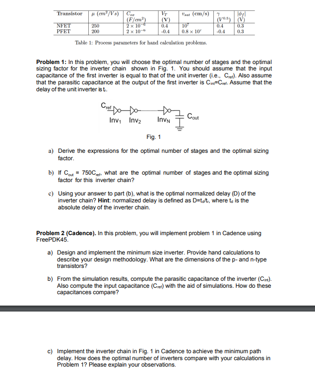
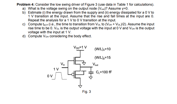
Transistor VT Vrat (cm/s) (cm'/V) Cor (F/cm) 250 2 x 10⁻⁴ 200 2 x 10⁻⁶ (V) NFET PFET 0.4 -0.4 107 0.8 x 10' (vos) ( 0.4 0.3 -0.4 0.3 Table 1: Process parameters for hand calculation problems. Problem 1: In this problem, you will choose the optimal number of stages and the optimal sizing factor for the inverter chain shown in Fig. 1. You should assume that the input capacitance of the first inverter is equal to that of the unit inverter (i.e., Cret). Also assume that the parasitic capacitance at the output of the first inverter is Cint=Cref. Assume that the delay of the unit inverter ist. Crefoto InVN Cout Invt Inv2 Fig. 1 a) Derive the expressions for the optimal number of stages and the optimal sizing factor. b) If Court = 750Cefo what are the optimal number of stages and the optimal sizing factor for this inverter chain? c) Using your answer to part (b), what is the optimal normalized delay (D) of the inverter chain? Hint: normalized delay is defined as Dets/t, where to is the absolute delay of the inverter chain. Problem 2 (Cadence). In this problem, you will implement problem 1 in Cadence using FreePDK45 a) Design and implement the minimum size inverter. Provide hand calculations to describe your design methodology. What are the dimensions of the p- and n-type transistors? b) From the simulation results, compute the parasitic capacitance of the inverter (Cint). Also compute the input capacitance (Cret) with the aid of simulations. How do these capacitances compare? c) Implement the inverter chain in Fig. 1 in Cadence to achieve the minimum path delay. How does the optimal number of inverters compare with your calculations in Problem 1? Please explain your observations. Problem 4: Consider the low swing driver of Figure 3 (use data in Table 1 for calculations). a) What is the voltage swing on the output node (Vout)? Assume y=0. b) Estimate (i) the energy drawn from the supply and (ii) energy dissipated for a 0 V to 1 V transition at the input. Assume that the rise and fall times at the input are 0. Repeat the analysis for a 1 V to 0 V transition at the input. c) Compute tpH (i.e., the time to transition from VoL to (VOH + VOL)/2). Assume the input rise time to be 0. VoL is the output voltage with the input at O V and Vow is the output voltage with the input at 1 V. d) Compute Vos considering the body effect. Vop=1 V (W/L)n=10 (W/L)p=15 Vin Vout 1 V CL=100 fF OV Fig. 3 Transistor VT Vrat (cm/s) (cm'/V) Cor (F/cm) 250 2 x 10⁻⁴ 200 2 x 10⁻⁶ (V) NFET PFET 0.4 -0.4 107 0.8 x 10' (vos) ( 0.4 0.3 -0.4 0.3 Table 1: Process parameters for hand calculation problems. Problem 1: In this problem, you will choose the optimal number of stages and the optimal sizing factor for the inverter chain shown in Fig. 1. You should assume that the input capacitance of the first inverter is equal to that of the unit inverter (i.e., Cret). Also assume that the parasitic capacitance at the output of the first inverter is Cint=Cref. Assume that the delay of the unit inverter ist. Crefoto InVN Cout Invt Inv2 Fig. 1 a) Derive the expressions for the optimal number of stages and the optimal sizing factor. b) If Court = 750Cefo what are the optimal number of stages and the optimal sizing factor for this inverter chain? c) Using your answer to part (b), what is the optimal normalized delay (D) of the inverter chain? Hint: normalized delay is defined as Dets/t, where to is the absolute delay of the inverter chain. Problem 2 (Cadence). In this problem, you will implement problem 1 in Cadence using FreePDK45 a) Design and implement the minimum size inverter. Provide hand calculations to describe your design methodology. What are the dimensions of the p- and n-type transistors? b) From the simulation results, compute the parasitic capacitance of the inverter (Cint). Also compute the input capacitance (Cret) with the aid of simulations. How do these capacitances compare? c) Implement the inverter chain in Fig. 1 in Cadence to achieve the minimum path delay. How does the optimal number of inverters compare with your calculations in Problem 1? Please explain your observations. Problem 4: Consider the low swing driver of Figure 3 (use data in Table 1 for calculations). a) What is the voltage swing on the output node (Vout)? Assume y=0. b) Estimate (i) the energy drawn from the supply and (ii) energy dissipated for a 0 V to 1 V transition at the input. Assume that the rise and fall times at the input are 0. Repeat the analysis for a 1 V to 0 V transition at the input. c) Compute tpH (i.e., the time to transition from VoL to (VOH + VOL)/2). Assume the input rise time to be 0. VoL is the output voltage with the input at O V and Vow is the output voltage with the input at 1 V. d) Compute Vos considering the body effect. Vop=1 V (W/L)n=10 (W/L)p=15 Vin Vout 1 V CL=100 fF OV Fig. 3
