

Answered step by step
Verified Expert Solution
Question
1 Approved Answer
PLEASE USE VERILOG in Vivado PLEASE USE VERILOG in Vivado PLEASE USE VERILOG in Vivado PLEASE USE VERILOG in Vivado PLEASE USE VERILOG in Vivado
PLEASE USE VERILOG in Vivado
PLEASE USE VERILOG in Vivado
PLEASE USE VERILOG in Vivado

PLEASE USE VERILOG in Vivado
PLEASE USE VERILOG in Vivado
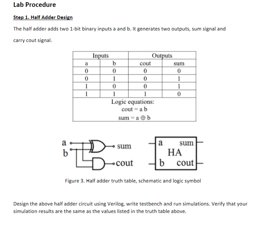
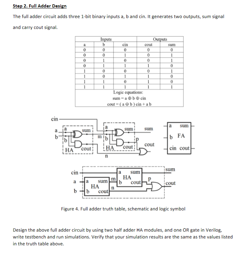
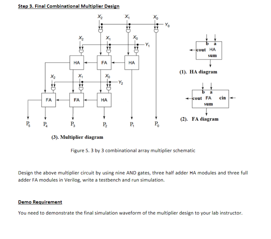
Part 1: 3 By 3 Binary Combinational Array Multiplier The binary combinational multiplier diagram: Figure 1.3 by 3 binary combinational multiplication diagram This lab is to design the above multiplier by using the hardware structure shown below: (). viumipier unagram Figure 2.3 by 3 binary combinational array multiplier hardware structure Step 1. Half Adder Design The half adder adds two 1-bit binary inputs a and b. It generates two outputs, sum signal and carry cout signal. Figure 3. Half adder truth table, schematic and logic symbol Design the above half adder circuit using Verilog, write testbench and run simulations. Verify that your simulation results are the same as the values listed in the truth table above. Step 2. Full Adder Design The full adder circuit adds three 1-bit binary inputs a, b and cin. It generates two outputs, sum signal and carry cout signal. Figure 4. Full adder truth table, schematic and logic symbol Design the above full adder circuit by using two half adder HA modules, and one OR gate in Verilog, write testbench and run simulations. Verify that your simulation results are the same as the values listed in the truth table above. Step 3. Final Combinational Multiplier Design (3). Multiplier diagram Figure 5.3 by 3 combinational array multiplier schematic Design the above multiplier circuit by using nine AND gates, three half adder HA modules and three full adder FA modules in Verilog, write a testbench and run simulation. Demo Requirement You need to demonstrate the final simulation waveform of the multiplier design to your lab instructor. Part 1: 3 By 3 Binary Combinational Array Multiplier The binary combinational multiplier diagram: Figure 1.3 by 3 binary combinational multiplication diagram This lab is to design the above multiplier by using the hardware structure shown below: (). viumipier unagram Figure 2.3 by 3 binary combinational array multiplier hardware structure Step 1. Half Adder Design The half adder adds two 1-bit binary inputs a and b. It generates two outputs, sum signal and carry cout signal. Figure 3. Half adder truth table, schematic and logic symbol Design the above half adder circuit using Verilog, write testbench and run simulations. Verify that your simulation results are the same as the values listed in the truth table above. Step 2. Full Adder Design The full adder circuit adds three 1-bit binary inputs a, b and cin. It generates two outputs, sum signal and carry cout signal. Figure 4. Full adder truth table, schematic and logic symbol Design the above full adder circuit by using two half adder HA modules, and one OR gate in Verilog, write testbench and run simulations. Verify that your simulation results are the same as the values listed in the truth table above. Step 3. Final Combinational Multiplier Design (3). Multiplier diagram Figure 5.3 by 3 combinational array multiplier schematic Design the above multiplier circuit by using nine AND gates, three half adder HA modules and three full adder FA modules in Verilog, write a testbench and run simulation. Demo Requirement You need to demonstrate the final simulation waveform of the multiplier design to your lab instructorStep by Step Solution
There are 3 Steps involved in it
Step: 1

Get Instant Access to Expert-Tailored Solutions
See step-by-step solutions with expert insights and AI powered tools for academic success
Step: 2

Step: 3
Ace Your Homework with AI
Get the answers you need in no time with our AI-driven, step-by-step assistance
Get Started
Pro Oracle Fusion Applications Installation And Administration
Authors: Tushar Thakker
1st Edition
1484209834, 9781484209837