Question: Pleases design below by using Cadence tool.. Coursework Assignment: Full Custom Design of a Digital to Analogue Converter (DAC) in 90nm/45nm CMOS Department of Electrical
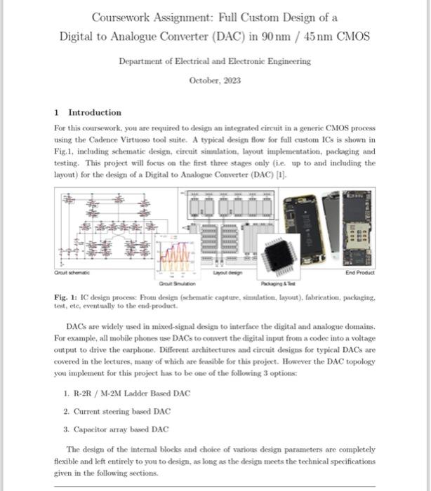
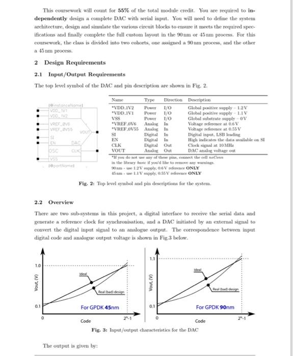
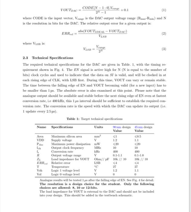
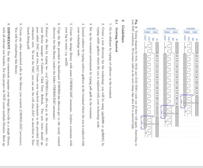
Coursework Assignment: Full Custom Design of a Digital to Analogue Converter (DAC) in 90nm/45nm CMOS Department of Electrical and Electronic Engineering October, 2023 1 Introduction For this coursework, you are required to design an integrated circuit in a generic CMOS process using the Cadence Virtuoso tool suite. A typical design flow for full custom ICs is shown in Fig.1, including schematic design, circuit simulation, layout implementation, packaging and testing. This project will focus on the first three stages only (i.e up to and including the layout) for the design of a Digital to Analogue Converter (DAC) [1]. Fig. 1: IC denign procese: Froti design (ochematic capture, simulation, layout), fabrication, packaging. tert, etc, everatually to the end-product. DACs are widely used in mixed-signal design to interface the digital and analogue douains. For example, all mobile photes use DACs to cotvert the digital input frotn a codec into a voltage output to drive the earphone. Different architectures and circuit designs for typical DACs are covered in the lectures, many of which are feasible for this project. However the DAC topology you implement for this project his to be one of the following 3 options: 1. R-2R / M-2M Ladder Based DAC 2. Current steering based DAC 3. Capacitor array based DAC The design of the internal blocks and choice of various design parameters are completely flexible and left entirely to you to design, as long as the design meets the technical specifications given in the following sections. This conrsework will comut for 55% of the total module credit. You are required to independently design a complete DAC with serial input. You will need to define the system architecture, design and simulate the varions circuit blocks to ensure it meets the required specifications and finally complete the full custom layout in the 90nm or 45nm process. For this coursework, the class is divided into two cohorts, one assigned a 90 man procese, and the other a 45mm process. 2 Design Requirements 2.1 Input/Output Requirements The top level symbol of the DAC and pin description are shown in Fig. 2. Fig. 2: Top kevel symbol and pin descriptions for the spotem. 2.2 Overview There are two sub-systems in this project, a digital interface to receive the serial data and generate a reference clock for syachronisation, and a DAC initiated by an external sigal to convert the digital input signal to an analogue output. The correspondence between input digital code and analogue output voltage is shown in Fig.3 below. Fig. 3: Input/ontpet characteristios for the DAC The output is given by: VOUTDAC=2N1CODE[N1:0],Vranex+0.1 where CODE is the imput vector, Vnuge is the DAC output voltage range (RmaxRmin) and N is the resolution in bits for the DAC. The relative output error for a given output is: ERRrel=VLSBabs(VOUTIDEALVOUTDAC) where VLSB is: VLSD=2NVrange 2.3 Technical Specifications The required technical specifications for the DAC are given in Table. 1, with the timing requirement shown in Fig. 4. The EN signal is active high for N(N is equal to the number of bits) clock cycles and used to indicate that the data on SI is valiel, and will be elocked in at each rising edge of CLK, with LSB first. During this time, VOUT can vary or remain stable. The time between the falling edge of EN and VOUT becoming valid (for a new input) has to be smaller than 1 ps. The abolute error is also examined at this point. Please note that the analogue output should be available and stable before the next rising edge of EN even at fastest conversion rate, i.e 400kHz, this 1, s interval should be sufficient to establish the required conversion rate. The conversion rate is the speed with which the DAC can update its output (i.e. 1 update every 2.51s). Table 1: Target techaical specifications Analogue results will be tested 1 ps after the falling edge of EX. See Fig. 4 for detail. The resolution is a design choice for the student. Only the following choices are allowed: 8,10 or 12 -bits. The load impedance for VOUT is extemal to the DAC and should not be inchuded imto your design. This should be added in the testbench schematic. Fig. 4: Timing diagran for 8-bit, 10-bit and 12-bit DACs (only ote of these will apply, depending on your DAC resolution). SI becounes valid on the next rising edge after EN is asserted high. 3 Guidelines 3.1 Getting Started 1. Go to nfslone by typing od nfwhome in the terminal. 2. Create a new directory for the technology you will be nsing (mpdk090 or gpdk045) by typing mbdir gpdlerr where the sox is replaced with your techaology node. 3. Set up the terminal cuviroument by typing pdis spel in the terminal. 4. Launch cadence by typing cadenoe gpdlerx in the terminal where the xxx is replaced with your technology node. 5. Create the design library with name CMOS23 DAC, taername, (replace yourname with your log in name, e.g. am23). 6. Copy the files provided in blackboard (CMOS23.slac filestar.gz) to the newly created directory for this library (under the folder CMOS23 DAC.nsername). 7. Extract the files by typing tar-anf CMOS23,dar files far-gz in the terminal. Go to your library manager in Cadence, Click View, Refresh. Two new views should appear called DAC, and stam DAC. Create your top-level schenatic in the provided DAC shematic view. To test the DAC, you can the the cell stim DAC as described in Testbench.Setup.pdf. 8. Create any other associated cells in the library you created (CMOS23 DAC-nsermame). Yot will be submitting this library. 9. IMPORTANT: For this coursework organize your design files/cells in a single library, with all relevant test benches. For this project do NOT create multiple libraries, Bark up your design when necessary, this can be dome by zipping the entire library, or creating a new backup cellview for each cell. After creating the design library, make sure you that the peovided top-level design cell (DAC) and stimulus (stim DAC) and all the cells you create are in the design library folder. The files and folders should look like as follows: - Folder you run cadence - CMOS23_DAC_username Design library - DAC * stim.DAC ... 3.2 A good design In general, circuit design is never perfect and always involves a number of trade-offs with no single, correct solution. For purposes of this coursework the following are expected (i.e. to achieve a good mark): - Ensure your design does the job required. First and fotemost, make sure you achieve what is asked before adding any extra functionality or going for a higher resolution. - Minimise power and area requirements. Less power consunption means an increased battery lifetime and less silicon area means lower cost. - Messy designs very rarely work, in particular when systems become more complicated. Keep your schematics and layouts tidy, so that they can be reviewed easily. - Clear, concise documentation can help others understand/follow your design as well as help you revise/reuse design in the future. It is ensential you lavep clear, consistent rocorts. 3.3 System Level Although you are required to choose the structure of your DAC frotn three options given perviously, there are a number of different possible implementations for each structure with bey design considetations that need to be made to meet the specification. You are cncouraged to go through lecture notes and textbooks [2,3,5], or [7,8] for a general introduction (if textbooks are unavailable from the library). It is highly recommended that before you dive into the schematic design, you first plan the high-level desigu architecturally (i.e. with pen and paper). This will belp you define your I/O's, internal data/control lines, signal types, etc, and to specify the detailed technical specification for each block. You should spend some time reading relevant literature (i.e. text books, course notes, publications) to review possible circuit topologies and ensure your design is realistic and can meet the top level specifications. Please bare in mind that many of the specifications listed in Table, 1 can siguificantly impact your design. For example: - The area will constrain the selection of both active and pasaive devices (i.e. component values and count), for example, a 0.8mm0.8mun capacitor is typically
Step by Step Solution
There are 3 Steps involved in it

Get step-by-step solutions from verified subject matter experts


