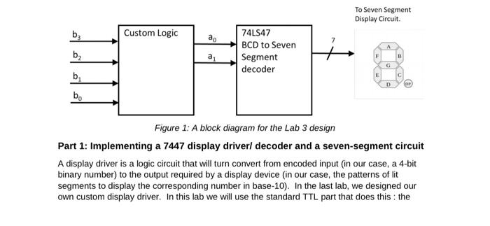
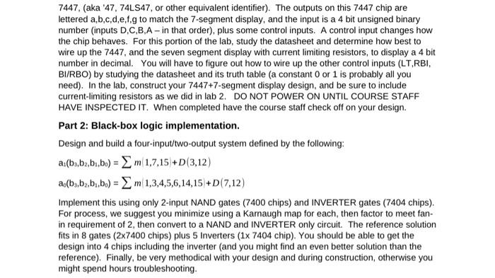
Prelab 1. Draw a simple chip level diagram of how you will wire up a 7447 BCD to Seven Segment decoder for this lab - document how you will connect all 16 pins. 2. Design the custom logic, as described below, circuit using a SOP form, you final design should be in terms of 2-input NAND and inverters for construction in 7400 and 7404 chips. To Seven Segment Display Circuit bz Custom Logic ao b2 74LS47 BCD to Seven Segment decoder a. G b. E D OP bo Figure 1: A block diagram for the Lab 3 design Part 1: Implementing a 7447 display driver decoder and a seven-segment circuit A display driver is a logic circuit that will turn convert from encoded input (in our case, a 4-bit binary number) to the output required by a display device in our case, the patterns of lit segments to display the corresponding number in base-10). In the last lab, we designed our own custom display driver. In this lab we will use the standard TTL part that does this: the 7447, (aka 47, 74LS47, or other equivalent identifier). The outputs on this 7447 chip are lettered a,b,c,d,e,f g to match the 7-segment display, and the input is a 4 bit unsigned binary number (inputs D,C,B,A - in that order), plus some control inputs. A control input changes how the chip behaves. For this portion of the lab, study the datasheet and determine how best to wire up the 7447, and the seven segment display with current limiting resistors, to display a 4 bit number in decimal. You will have to figure out how to wire up the other control inputs (LT, RBI, BI/RBO) by studying the datasheet and its truth table (a constant 0 or 1 is probably all you need). In the lab, construct your 7447+7-segment display design, and be sure to include current-limiting resistors as we did in lab 2. DO NOT POWER ON UNTIL COURSE STAFF HAVE INSPECTED IT. When completed have the course staff check off on your design. Part 2: Black-box logic implementation. Design and build a four-input/two-output system defined by the following: a:(b.ba,bubo) = m 1,7,15+D(3,12) ao(bs,b2,bu,bo) = m 1,3,4,5,6,14,15 +D(7,12) Implement this using only 2-input NAND gates (7400 chips) and INVERTER gates (7404 chips). For process, we suggest you minimize using a Karnaugh map for each, then factor to meet fan- in requirement of 2, then convert to a NAND and INVERTER only circuit. The reference solution fits in 8 gates (2x7400 chips) plus 5 Inverters (1x 7404 chip). You should be able to get the design into 4 chips including the inverter (and you might find an even better solution than the reference). Finally, be very methodical with your design and during construction, otherwise you might spend hours troubleshooting


