Question
PROJECT 1 Title: Arithmetic Logic Unit (ALU) Point Value: 100 The Problem In this project, you will be completing the design of a simple Arithmetic
PROJECT 1
Title: Arithmetic Logic Unit (ALU)
Point Value: 100
The Problem
In this project, you will be completing the design of a simple Arithmetic Logic Unit using Xilinx ISE Schematic Capture.
DISCLAIMER: The processor we are working with is a very basic 8 bit single cycle processor with no data memory. While it is a good representation and is good for education, commercial processors are typically more complex.
A skeleton has been provided that contains various aspects of the processor already designed. Below is a description of the ALU as it pertains to this processor. You will need to use these descriptions as well as the information in the architecture section to complete this design.
Arithmetic Logic Unit (ALU):
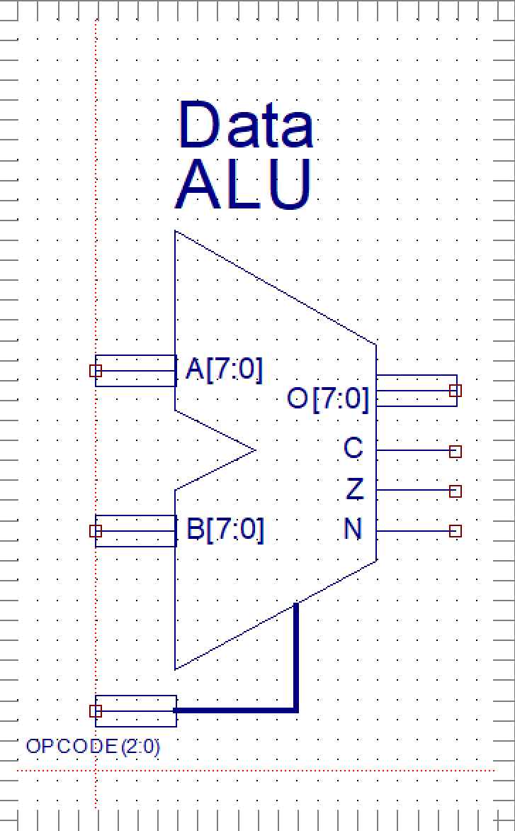
As covered in class, the arithmetic unit does the arithmetic and logic lifting for the processor. This ALU is an 8 bit ALU and can do 8 different operations as described in the table below. You will build the components for these logic and arithmetic operations.

| Opcode | Operation |
| 000 | O = B |
| 001 | O = A ^ B (bitwise xor) |
| 010 | O = A AND B (bitwise and) |
| 011 | O = A OR B (bitwise or) |
| 100 | O = A + B (addition) |
| 101 | O = A - B (subtract) |
| 110 | O(7) = 0, 0(6:0) = B (7:1) (logical shift right) |
| 111 | O = A * B (multiplication) |
ALU inputs: A(7:0):
8 bit data to be operated on. This comes from the register file, read data a(R_data_a).
B (7:0):
8 bit data to be operated on. This can come from the register file, read data b (R_data_b) or the data input to the processor.
Opcode (2:0): This picks the operation to be done. The opcode comes from instruction bits 6 down to 4.
ALU Outputs:
O (7:0):
The result of the ALU operation.
Testing
It is encouraged that you test your work as you go along. To aide in this, the skeleton comes with a test bench (simulation file) that you can use to test your designs.
ALU Test Bench
The ALU Test bench is labelled: ALU_ALU_sch_tb
This testbench steps through all the opcode values in order starting from 000 up to 111.
The values for A and B are currently both set to the binary value 10101010.
To use the text bench:
- Run the simulation as you would normally.
- Check the output for the opcode you are currently testing against the output (O).
- For example, if I have built the adder and I would like to test it, then I would put adder component output to input 4 (100) of my mux and run the test bench. I would then check the output value (0) when the opcode is 100. The output should be the result of adding 101010102 + 101010102.
You do not need to have all the components built in the ALU to test an individual one, but you do need to have the multiplexor component built at the very least before you can test the rest of the components.
Implementation Details & Hints:
- You can work in groups of 1-2 students.
- Review the Architecture Section.
- You must use schematics. You CANNOT use VHDL or Verilog in your design.
- You should design using components. Build and design the components one step at a time from the bottom up.
- You cannot use any of the inbuilt adders, subtractors or other xilinx arithmetic built in components. Flip flops (FD/FDE), D- Latches(LD), Multiplexors and decoders are ok.
- You CANNOT use the multi bit flip flops
- You CANNOT use the Mux8_8, reg16 or reg2 components
- Any multibit component needed has to be built by you
- Note: The multiplexors in xilinx are all 1 bit multiplexors so you need to build an 8 bit multiplexor out of these
- DO NOT change the inputs or outputs in the skeleton.
- DO NOT change any of the schematics outside of the ones required for the project.
- If you make any changes, redownload the skeleton and copy your work over as needed.
- You will need to zip up the entire folder your project is located in and submit it on blackboard
- If you worked alone you should label the zip file as: lastname_firstname_project1.zip
- If you worked as a team label the zip file as: lastname_firstname_lastname_firstname_project1.zip
- Any late submissions will incur a penalty of 10 points per every 6 hours they are late.
Connecting a bit from one bus to a bit of a different bus in Xilinx:
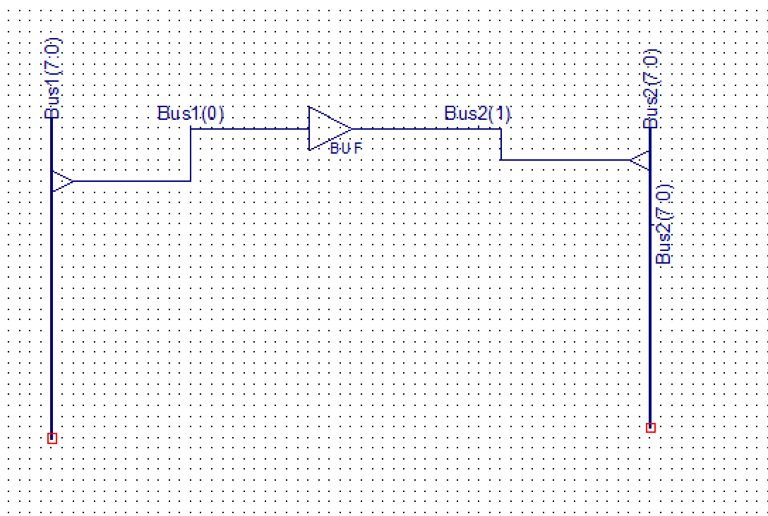
Connecting a bit from one bus to a bit of a different bus in xilinx can be an issue. In order to do this, you need a buffer component (buf in xilinx).
- You need to put a bus tap from the the source bus.
- Draw a wire from the bus tap to the input of the buf component.
- Draw a wire from the buf to the bus tap of the second bus.
- Then you just need to name those wires to reflect what bit they are connected to.
See the picture below for an example, in this picture I am connecting the bit 0 of Bus1 to bit 1 of Bus2.

Grading Breakdown:
The 100 total points for this part will be broken down into expected functionality, and how organized the design is.
- [80] **Design functionality:
- [5] O = B
- [8] Xor
- [8] AND
- [8] OR
- [13] Adder
- [15] Subtracter
- [8] Shift
- [15] Multiply
- [20] Style and Submission
- [8] Use of components
- [2] Schematic is organized and easy to follow
- [10] Followed submission requirements
**If the 8 bit multiplexor component in the ALU does not work you will lose 20 points on the Design Functionality (in addition to any other points you lose).
Arithmetic Logic Unit(GPP) Architecture:
This section describes the architecture for the GPP that will be used in this project. As outlined earlier, this is a very simple processor.
Arithmetic Logic Unit (ALU):
The ALU for this processor is an 8 bit ALU and can perform 8 operations as described in the table below.

| Opcode | Operation | Description |
| 000 | O = B | Output is = equal to input B |
| 001 | O = A ^ B (bitwise xor) | Xor of each bit in A with the corresponding bit in B |
| 010 | O = A AND B (bitwise and) | AND of each bit in A with the corresponding bit in B |
| 011 | O = A OR B (bitwise or) | OR of each bit in A with the corresponding bit in B |
| 100 | O = A + B (addition) | 8 bit addition with a final carry out bit |
| 101 | O = A - B (subtract) | 8 bit subtraction with a borrow out bit |
| 110 | O(7) = 0, 0(6:0) = B (7:1) (logical shift right) | Logical shift of the data at input B right by one bit |
| 111 | O = A * B (multiplication) | 8 Multiplication. To make our design simpler, we will only keep the lower 8 bits of the result and signal an overflow |
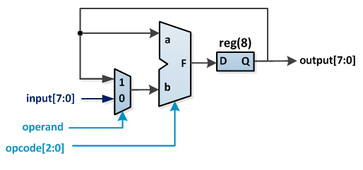
The B input for the ALU will take an address from a register or the input input. The input-input is the I/O input for this processor. It takes 8 bit data from the outside and feeds it into the ALU. This data will be used for operations or fed into a register and is chosen by the operand select signal. This is also the use-input bit in the machine code for the instruction.
. . . . . . . . . . . . . . . . . . . . . . . . . . . . . . . . . . . . OP CODE (2:0) . :: . . . : : . . : . : : : : : : : : : : :: B[7:0] : : : N ALU Data : :: : : . : : : : : : : : : : : : : : : : . . . . . . . . . . . . . . . . . / . : A[7:0] : 0[7:0] . : : : : : : : : : : / .. . . . . . . . .. : : : : : : : : : : : : : . ZNO.0. : . . : . : : : : : : : : : : : : : : : : : : : : : : : : : : : : : : : : . ]: []. . . . : .. : : : : : : : : : : : : : : : : : : : : : : : : : : : : : : : : : . : : . . . . . . . . . . . . . . . . . . . . . . . . . . . . . . . . . . . . . . . . . . . . . . . . . . . . . . . . . . . . . . . . . . . . . . . . . . . . . . . . . . . . . . . . . . . . . . . . . . . . . . . . . . . . . . . . . . . . . . . . . . . . . . . . . . . . . . . . . . . . . . . . . . . . . . . . . . . . . . . . . . . . . . . . . . . . . . . . . . . : Bus2(70) . . . . . . . . . . . . T 1 [ . . . . . . . . . . . . . . . . . . . . . . . . . 9 1 H . ' ' ' ' F (0 sng . . . . . . . . . . 1 7 C . . . . . . . . . . . . . . . . . 11 IH . . . . . . . sng ::::: . Bus270):::: Bus1(7:0)... reg(8) SFD 01 output[7:0] input[7:0] operand opcode(2:0) . . . . . . . . . . . . . . . . . . . . . . . . . . . . . . . . . . . . OP CODE (2:0) . :: . . . : : . . : . : : : : : : : : : : :: B[7:0] : : : N ALU Data : :: : : . : : : : : : : : : : : : : : : : . . . . . . . . . . . . . . . . . / . : A[7:0] : 0[7:0] . : : : : : : : : : : / .. . . . . . . . .. : : : : : : : : : : : : : . ZNO.0. : . . : . : : : : : : : : : : : : : : : : : : : : : : : : : : : : : : : : . ]: []. . . . : .. : : : : : : : : : : : : : : : : : : : : : : : : : : : : : : : : : . : : . . . . . . . . . . . . . . . . . . . . . . . . . . . . . . . . . . . . . . . . . . . . . . . . . . . . . . . . . . . . . . . . . . . . . . . . . . . . . . . . . . . . . . . . . . . . . . . . . . . . . . . . . . . . . . . . . . . . . . . . . . . . . . . . . . . . . . . . . . . . . . . . . . . . . . . . . . . . . . . . . . . . . . . . . . . . . . . . . . . : Bus2(70) . . . . . . . . . . . . T 1 [ . . . . . . . . . . . . . . . . . . . . . . . . . 9 1 H . ' ' ' ' F (0 sng . . . . . . . . . . 1 7 C . . . . . . . . . . . . . . . . . 11 IH . . . . . . . sng ::::: . Bus270):::: Bus1(7:0)... reg(8) SFD 01 output[7:0] input[7:0] operand opcode(2:0)
Step by Step Solution
There are 3 Steps involved in it
Step: 1

Get Instant Access to Expert-Tailored Solutions
See step-by-step solutions with expert insights and AI powered tools for academic success
Step: 2

Step: 3

Ace Your Homework with AI
Get the answers you need in no time with our AI-driven, step-by-step assistance
Get Started


