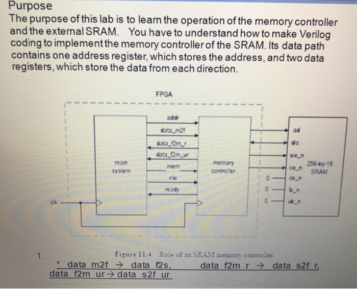
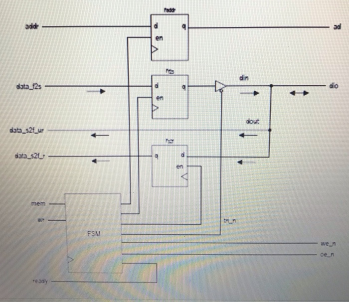
Purpose The purpose of this lab is to learn the operation of the memory controller and the external SRAM. You have to understand how to make Verilog coding to implement the memory controller of the SRAM. Its data path contains one address register, which stores the address, and two data registers, which store the data from each direction. FPGA 30 data_m24 data_f2m_ data_f2m_u mem min system memory controller 256-by-16 SRAM Figure 11.+ Role of an SRAM memory controller * data m2f = data f2s, data f2mr data s2fr. data f2m ur data s2f ur data_325 data_52f_up diata_s23 mem rey Preparation 1. Designing the input/output and the operation of memory controller. 2. Drawing State Diagram or ASM chart. 3. Writing the Verilog code of the circuit you want to implement, 4. Simulating the Verilog code using a simulator to check if it is working well. 5. Synthesizing the Verilog code using a tool form Xilinx so that it can be programmed onto an FPGA 6. Programming the FPGA (a Spartan3E series FPGA from Xilinx) on the lab board 7. Applying inputs to and observing outputs from our circuit using the peripherals (like switches, buttons, LEDs, etc) on the board Equipment & Tools Xilinx ISE 14.7 ISE Simulator(ISIM) Spartan-3 Starter Board A) simulation of Memory controller (Feb. 13): refer to List 11.1 1. Use 18bits of address(00 0001 0001 0001 0001), 16bits of data(0011 0011 0011 0011), 2. Initial condition mem:0, w: 1, 3. Write input mem: 1, w:0, addr, output ad, dio a, wen, oen, ready 4. Read: input mem:1, rw 1, dio a, addr, output ad, we noen data_s2f_ur, data_s2f_r, ready Default oe_n = 1; we_n = 1; tri_n = 1; ready = 0 - - - - ready = 1 memast 72 Solar 1 - dals PO: --data_f2s W=31 to Post aadr add: data_f2s oe_n = 0 we_n = 0 trin = 0 ce_n = 0 - do Figure 11.6 ASMD chart of a safe SRAM controller. B) implementation of Memory controller to S3 board (Feb. 18): refer to List 11.2 1. sw. It is 8 bits wide and used as data or address input 2. LED. It is 8 bit wide and used to display the retrieved data. 3. btn[0]. When it is asserted, the current value of sw is loaded to a data register, The output of the register is used as the data input for the write operation. 4. btn[1]. When it is asserted, the controller uses the value of sw as a memory address and performs a write operation. 5. btn[2]. When it is asserted, the controller uses the value of sw as a memory address and performs a read operation. The readout is routed to the LED signal. 6. SW (0100 0001), btn_0. SW: (0000 1110), btn_1. Sw:(0100 0011). btn_0.SW: (0000 1111), btn_1. SW :( 0000 1110), btn_2 (data s2f 0100 0001) sw: (0000 1110), btn_2. (data_s2f: 0000 1111) Purpose The purpose of this lab is to learn the operation of the memory controller and the external SRAM. You have to understand how to make Verilog coding to implement the memory controller of the SRAM. Its data path contains one address register, which stores the address, and two data registers, which store the data from each direction. FPGA data_m24 data_mu datam memory 256-by-16 em Figure 11.4 Role of an SRAM memory controller. * data_m2f data_f2s,_ data_f2m_r data_s2f_r, data_f2m_ur data_s2f_ur adid data_2 data_2_ 52 data_s2f_r, data_f2m_ur data_s2f_ur doto_324 Figure 11.5 Block diagram of a memory controller Preparation 1. Designing the input/output and the operation of memory controller. 2. Drawing State Diagram or ASM chart. 3. Writing the Verilog code of the circuit you want to implement 4. Simulating the Verilog code using a simulator to check if it is working well. 5. Synthesizing the Verilog code using a tool form Xilinx so that it can be programmed onto an FPGA 6. Programming the FPGA (a Spartan3E series FPGA from Xilinx) on the lab board. 7. Applying inputs to and observing outputs from our circuit using the peripherals (like switches, buttons, LEDs, etc) on the board Equipment & Tools Xilinx ISE 14.7 ISE Simulator(ISIM) Spartan-3 Starter Board A) simulation of Memory controller (Feb. 13): refer to List 11.1 1. Use 18bits of address(00 0001 0001 0001 0001), 16bits of data(0011 0011 0011 0011), 2. Initial condition: mem:0, rw: 1, 3. Write: input: mem:1, rw:0, addr, output: ad, dio_a, we_n, oe_n, ready 4. Read: input: mem:1, rw:1, dio_a, addr, output: ad., we_n, oe_n, data_s2f_ur, data_s2f_r, ready Default on=1; wen= 1; tint; ready = 0 ready = 1 Den te =0 5. Figure 11.6 ASMD chart of a safe SRAM controller B) implementation of Memory controller to S3 board (Feb. 18): refer to List 11.2 1. sw. It is 8 bits wide and used as data or address input 2. LED. It is 8 bit wide and used to display the retrieved data. 3. btn[0]. When it is asserted, the current value of sw is loaded to a data register, The output of the register is used as the data input for the write operation. 4. btn[1]. When it is asserted, the controller uses the value of sw as a memory address and performs a write operation. 5. btn[2]. When it is asserted, the controller uses the value of sw as a memory address and performs a read operation. The readout is routed to the LED signal. 6. SW (0100 0001), btn 0, SW: (0000 1110). btn_1, SW (0100 0011), btn_0, SW: (0000 1111), btn_1, SW :( 0000 1110), btn_2,(data_s2f: 0100 0001) sw: (0000 1110), btn_2, (data_s2f: 0000 1111) Deliverables Purpose The purpose of this lab is to learn the operation of the memory controller and the external SRAM. You have to understand how to make Verilog coding to implement the memory controller of the SRAM. Its data path contains one address register, which stores the address, and two data registers, which store the data from each direction. FPGA 30 data_m24 data_f2m_ data_f2m_u mem min system memory controller 256-by-16 SRAM Figure 11.+ Role of an SRAM memory controller * data m2f = data f2s, data f2mr data s2fr. data f2m ur data s2f ur data_325 data_52f_up diata_s23 mem rey Preparation 1. Designing the input/output and the operation of memory controller. 2. Drawing State Diagram or ASM chart. 3. Writing the Verilog code of the circuit you want to implement, 4. Simulating the Verilog code using a simulator to check if it is working well. 5. Synthesizing the Verilog code using a tool form Xilinx so that it can be programmed onto an FPGA 6. Programming the FPGA (a Spartan3E series FPGA from Xilinx) on the lab board 7. Applying inputs to and observing outputs from our circuit using the peripherals (like switches, buttons, LEDs, etc) on the board Equipment & Tools Xilinx ISE 14.7 ISE Simulator(ISIM) Spartan-3 Starter Board A) simulation of Memory controller (Feb. 13): refer to List 11.1 1. Use 18bits of address(00 0001 0001 0001 0001), 16bits of data(0011 0011 0011 0011), 2. Initial condition mem:0, w: 1, 3. Write input mem: 1, w:0, addr, output ad, dio a, wen, oen, ready 4. Read: input mem:1, rw 1, dio a, addr, output ad, we noen data_s2f_ur, data_s2f_r, ready Default oe_n = 1; we_n = 1; tri_n = 1; ready = 0 - - - - ready = 1 memast 72 Solar 1 - dals PO: --data_f2s W=31 to Post aadr add: data_f2s oe_n = 0 we_n = 0 trin = 0 ce_n = 0 - do Figure 11.6 ASMD chart of a safe SRAM controller. B) implementation of Memory controller to S3 board (Feb. 18): refer to List 11.2 1. sw. It is 8 bits wide and used as data or address input 2. LED. It is 8 bit wide and used to display the retrieved data. 3. btn[0]. When it is asserted, the current value of sw is loaded to a data register, The output of the register is used as the data input for the write operation. 4. btn[1]. When it is asserted, the controller uses the value of sw as a memory address and performs a write operation. 5. btn[2]. When it is asserted, the controller uses the value of sw as a memory address and performs a read operation. The readout is routed to the LED signal. 6. SW (0100 0001), btn_0. SW: (0000 1110), btn_1. Sw:(0100 0011). btn_0.SW: (0000 1111), btn_1. SW :( 0000 1110), btn_2 (data s2f 0100 0001) sw: (0000 1110), btn_2. (data_s2f: 0000 1111) Purpose The purpose of this lab is to learn the operation of the memory controller and the external SRAM. You have to understand how to make Verilog coding to implement the memory controller of the SRAM. Its data path contains one address register, which stores the address, and two data registers, which store the data from each direction. FPGA data_m24 data_mu datam memory 256-by-16 em Figure 11.4 Role of an SRAM memory controller. * data_m2f data_f2s,_ data_f2m_r data_s2f_r, data_f2m_ur data_s2f_ur adid data_2 data_2_ 52 data_s2f_r, data_f2m_ur data_s2f_ur doto_324 Figure 11.5 Block diagram of a memory controller Preparation 1. Designing the input/output and the operation of memory controller. 2. Drawing State Diagram or ASM chart. 3. Writing the Verilog code of the circuit you want to implement 4. Simulating the Verilog code using a simulator to check if it is working well. 5. Synthesizing the Verilog code using a tool form Xilinx so that it can be programmed onto an FPGA 6. Programming the FPGA (a Spartan3E series FPGA from Xilinx) on the lab board. 7. Applying inputs to and observing outputs from our circuit using the peripherals (like switches, buttons, LEDs, etc) on the board Equipment & Tools Xilinx ISE 14.7 ISE Simulator(ISIM) Spartan-3 Starter Board A) simulation of Memory controller (Feb. 13): refer to List 11.1 1. Use 18bits of address(00 0001 0001 0001 0001), 16bits of data(0011 0011 0011 0011), 2. Initial condition: mem:0, rw: 1, 3. Write: input: mem:1, rw:0, addr, output: ad, dio_a, we_n, oe_n, ready 4. Read: input: mem:1, rw:1, dio_a, addr, output: ad., we_n, oe_n, data_s2f_ur, data_s2f_r, ready Default on=1; wen= 1; tint; ready = 0 ready = 1 Den te =0 5. Figure 11.6 ASMD chart of a safe SRAM controller B) implementation of Memory controller to S3 board (Feb. 18): refer to List 11.2 1. sw. It is 8 bits wide and used as data or address input 2. LED. It is 8 bit wide and used to display the retrieved data. 3. btn[0]. When it is asserted, the current value of sw is loaded to a data register, The output of the register is used as the data input for the write operation. 4. btn[1]. When it is asserted, the controller uses the value of sw as a memory address and performs a write operation. 5. btn[2]. When it is asserted, the controller uses the value of sw as a memory address and performs a read operation. The readout is routed to the LED signal. 6. SW (0100 0001), btn 0, SW: (0000 1110). btn_1, SW (0100 0011), btn_0, SW: (0000 1111), btn_1, SW :( 0000 1110), btn_2,(data_s2f: 0100 0001) sw: (0000 1110), btn_2, (data_s2f: 0000 1111) Deliverables


