Answered step by step
Verified Expert Solution
Question
1 Approved Answer
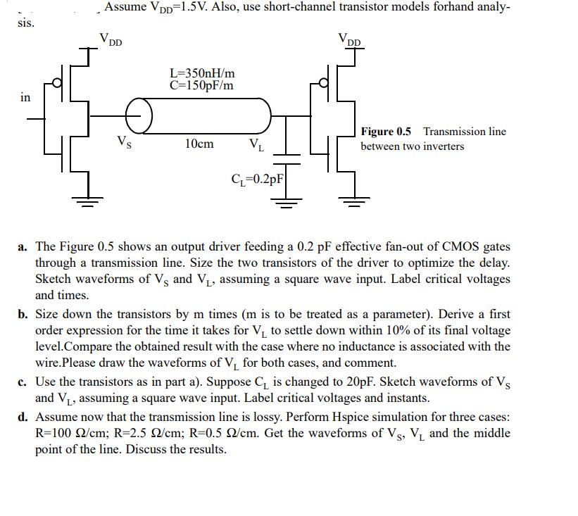
sis. in Assume VDD=1.5V. Also, use short-channel transistor models forhand analy- V DD Vs L=350nH/m C=150pF/m 10cm VL CL=0.2pF Vn Figure 0.5 Transmission line

sis. in Assume VDD=1.5V. Also, use short-channel transistor models forhand analy- V DD Vs L=350nH/m C=150pF/m 10cm VL CL=0.2pF Vn Figure 0.5 Transmission line between two inverters a. The Figure 0.5 shows an output driver feeding a 0.2 pF effective fan-out of CMOS gates through a transmission line. Size the two transistors of the driver to optimize the delay. Sketch waveforms of Vs and V, assuming a square wave input. Label critical voltages and times. b. Size down the transistors by m times (m is to be treated as a parameter). Derive a first order expression for the time it takes for V to settle down within 10% of its final voltage level. Compare the obtained result with the case where no inductance is associated with the wire.Please draw the waveforms of V for both cases, and comment. c. Use the transistors as in part a). Suppose C is changed to 20pF. Sketch waveforms of Vs and V, assuming a square wave input. Label critical voltages and instants. d. Assume now that the transmission line is lossy. Perform Hspice simulation for three cases: R=100 22/cm; R=2.5 /cm; R=0.5 /cm. Get the waveforms of VS, V and the middle point of the line. Discuss the results.
Step by Step Solution
★★★★★
3.48 Rating (161 Votes )
There are 3 Steps involved in it
Step: 1

Get Instant Access to Expert-Tailored Solutions
See step-by-step solutions with expert insights and AI powered tools for academic success
Step: 2

Step: 3

Ace Your Homework with AI
Get the answers you need in no time with our AI-driven, step-by-step assistance
Get Started


