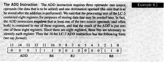
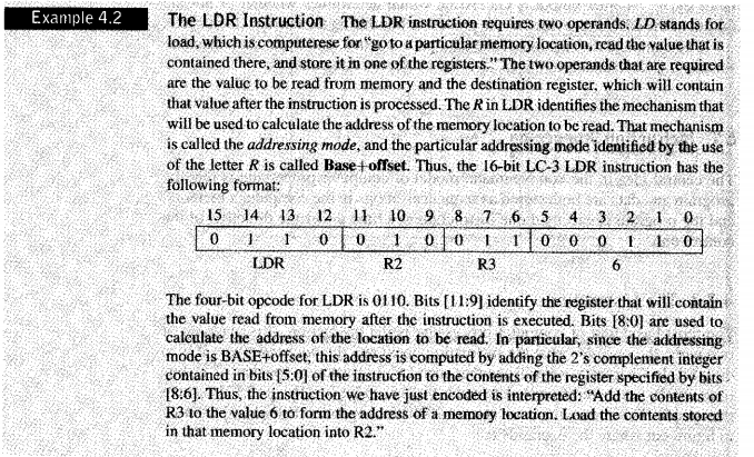
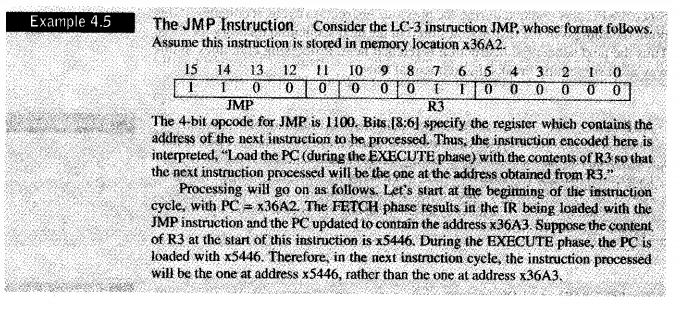
Study Examples 4.1, 4.2, and 4.5 in the text. Now do exactly the same analysis (using the same reasoning and the same format) for the instruction BRnzp in LC-3. You will need to know the exact meaning and functioning of the NZP condition codes to do this


C ARAVAN Example 4.1 The ADD Instruction The ADD instruction requires three operands: two source operands (the data that is to be added) and one destination operand (the sum that is to be stored after the addition is performed). We said that the processing unit of the LC-3 contained eight registers for purposes of storing data that may be needed later. In fact, the ADD instruction requires that at least one of the two source operands (and often both) is contained in one of these registers, and that the result of the ADD is put into one of these eight registers. Since there are eight registers, three bits are necessary to identify each register. Thus the 16-bit LC-3 ADD instruction has the following form (we say format): SUB 15 14 13 12 11 10 9 8 7 6 5 4 3 2 1 0 10 0 0 T L 1 0 1 0 1 0 0 0 0 1 1 0 1 ADDR6 R6 The 4-bit opcode for ADD, contained in bits [15:12], is 0001. Bits (11:91 identify the location to be used for storing the result, in this case register 6 (R6). Bits [8:6) and bits [2:0) identify the registers to be used to obtain the source operands, in this case R2 and R6. Bits (5:3) have a purpose that it is not necessary to understand in the context of this example. We will save the explanation of bits 15:31 for Section 5.2. Thus, the instruction we have just encoded is interpreted, "Add the contents of register 2 (R2) to the contents of register 6 (R6) and store the result back into register 6 (R6)." DOES Example 4.2 The LDR Instruction The LDR instruction requires two operands, LD stands for load, which is computerese for "go to a particular memory location, read the value that is contained there, and store it in one of the registers." The two operands that are required are the value to be read from memory and the destination register, which will contain that value after the instruction is processed. The Rin LDR identifies the mechanism that will be used to calculate the address of the memory location to be read. That mechanism is called the addressing mode, and the particular addressing mode identified by the use of the letter R is called Base+offset. Thus, the 16-bit LC-3 LDR instruction has the following format: 15 14 13 12 11 10 9 8 7 6 5 4 3 2 1 0 10 1 1 0 0 1 0 0 1 0 0 0 LDR R2 R3 A MARELA The four-bit opcode for LDR is 0110. Bits (11:9) identify the register that will contain the value read from memory after the instruction is executed. Bits 18:01 are used to calculate the address of the location to be read. In particular, since the addressing mode is BASE+offset, this address is computed by adding the 2's complement integer contained in bits (5:01 of the instruction to the contents of the register specified by bits [8:6). Thus, the instruction we have just encoded is interpreted: "Add the contents of R3 to the value 6 to form the address of a memory location. Lead the contents stored in that memory location into R2." Example 4.5 R3 The JMP Instruction Consider the LC-3 instruction JMP, whose format follows.. Assume this instruction is stored in memory location x36A2. 15 14 13 12 11 10 9 8 7 6 5 4 3 2 1 0 IT 1001010010 110 0 0 0 0 0 JMP The 4-bit opcode for JMP is 1100. Bits (8:6] specify the register which contains the address of the next instruction to be processed. Thus, the instruction encoded here is interpreted, "Load the PC (during the EXECUTE phase) with the contents of R3 so that the next instruction processed will be the one at the address obtained from R3." Processing will go on as follows. Let's start at the beginning of the instruction cycle, with PC = 36A2. The FETCH phase results in the IR being loaded with the JMP instruction and the PC updated to contain the address x36A3. Suppose the content of R3 at the start of this instruction is x5446. During the EXECUTE phase, the PC is loaded with x5446. Therefore, in the next instruction cycle, the instruction processed will be the one at address x5446, rather than the one at address X36A3. AS T C ARAVAN Example 4.1 The ADD Instruction The ADD instruction requires three operands: two source operands (the data that is to be added) and one destination operand (the sum that is to be stored after the addition is performed). We said that the processing unit of the LC-3 contained eight registers for purposes of storing data that may be needed later. In fact, the ADD instruction requires that at least one of the two source operands (and often both) is contained in one of these registers, and that the result of the ADD is put into one of these eight registers. Since there are eight registers, three bits are necessary to identify each register. Thus the 16-bit LC-3 ADD instruction has the following form (we say format): SUB 15 14 13 12 11 10 9 8 7 6 5 4 3 2 1 0 10 0 0 T L 1 0 1 0 1 0 0 0 0 1 1 0 1 ADDR6 R6 The 4-bit opcode for ADD, contained in bits [15:12], is 0001. Bits (11:91 identify the location to be used for storing the result, in this case register 6 (R6). Bits [8:6) and bits [2:0) identify the registers to be used to obtain the source operands, in this case R2 and R6. Bits (5:3) have a purpose that it is not necessary to understand in the context of this example. We will save the explanation of bits 15:31 for Section 5.2. Thus, the instruction we have just encoded is interpreted, "Add the contents of register 2 (R2) to the contents of register 6 (R6) and store the result back into register 6 (R6)." DOES Example 4.2 The LDR Instruction The LDR instruction requires two operands, LD stands for load, which is computerese for "go to a particular memory location, read the value that is contained there, and store it in one of the registers." The two operands that are required are the value to be read from memory and the destination register, which will contain that value after the instruction is processed. The Rin LDR identifies the mechanism that will be used to calculate the address of the memory location to be read. That mechanism is called the addressing mode, and the particular addressing mode identified by the use of the letter R is called Base+offset. Thus, the 16-bit LC-3 LDR instruction has the following format: 15 14 13 12 11 10 9 8 7 6 5 4 3 2 1 0 10 1 1 0 0 1 0 0 1 0 0 0 LDR R2 R3 A MARELA The four-bit opcode for LDR is 0110. Bits (11:9) identify the register that will contain the value read from memory after the instruction is executed. Bits 18:01 are used to calculate the address of the location to be read. In particular, since the addressing mode is BASE+offset, this address is computed by adding the 2's complement integer contained in bits (5:01 of the instruction to the contents of the register specified by bits [8:6). Thus, the instruction we have just encoded is interpreted: "Add the contents of R3 to the value 6 to form the address of a memory location. Lead the contents stored in that memory location into R2." Example 4.5 R3 The JMP Instruction Consider the LC-3 instruction JMP, whose format follows.. Assume this instruction is stored in memory location x36A2. 15 14 13 12 11 10 9 8 7 6 5 4 3 2 1 0 IT 1001010010 110 0 0 0 0 0 JMP The 4-bit opcode for JMP is 1100. Bits (8:6] specify the register which contains the address of the next instruction to be processed. Thus, the instruction encoded here is interpreted, "Load the PC (during the EXECUTE phase) with the contents of R3 so that the next instruction processed will be the one at the address obtained from R3." Processing will go on as follows. Let's start at the beginning of the instruction cycle, with PC = 36A2. The FETCH phase results in the IR being loaded with the JMP instruction and the PC updated to contain the address x36A3. Suppose the content of R3 at the start of this instruction is x5446. During the EXECUTE phase, the PC is loaded with x5446. Therefore, in the next instruction cycle, the instruction processed will be the one at address x5446, rather than the one at address X36A3. AS T
