The 74155 Decoder IC can be configured as a dual 2-to-4-line decoder or as a single 3-to-8-line decoder. Schematic diagram of the 74155 Decoder
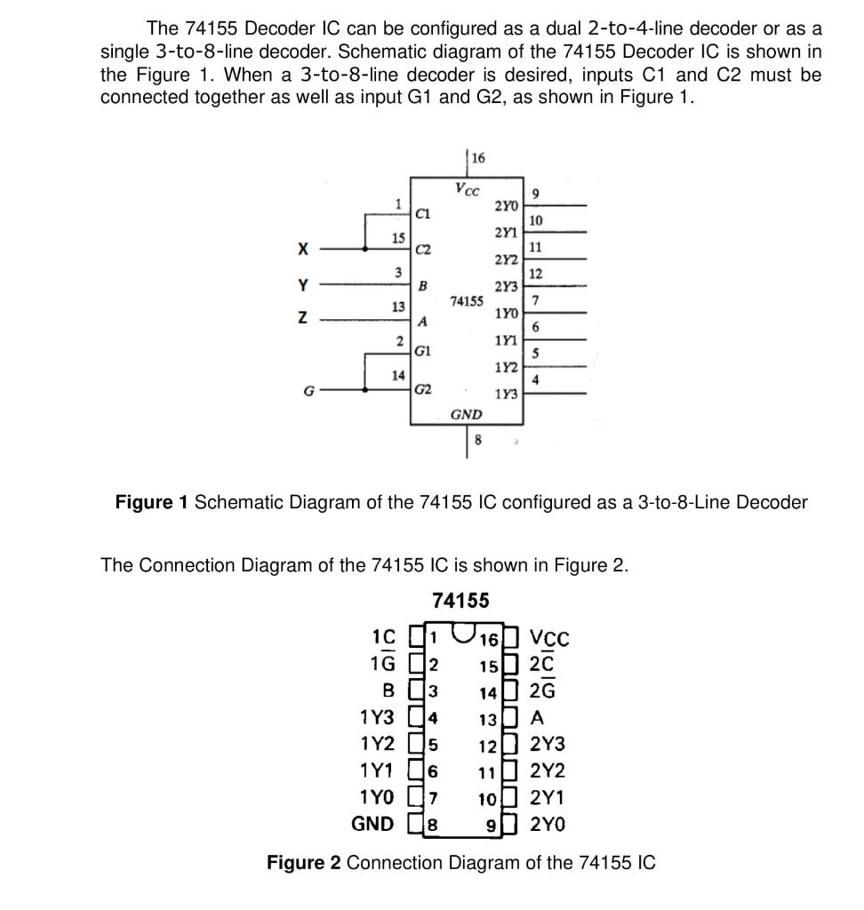
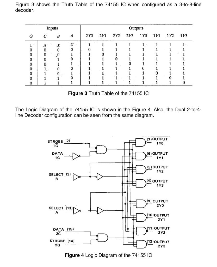
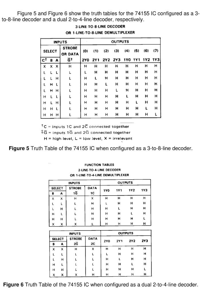
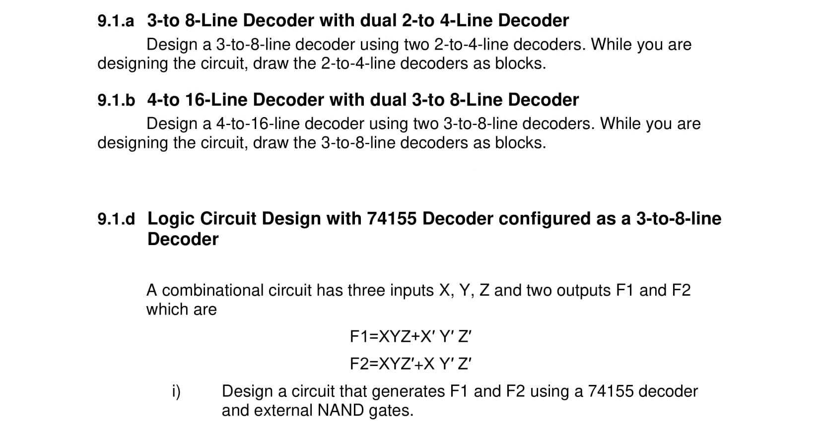
The 74155 Decoder IC can be configured as a dual 2-to-4-line decoder or as a single 3-to-8-line decoder. Schematic diagram of the 74155 Decoder IC is shown in the Figure 1. When a 3-to-8-line decoder is desired, inputs C1 and C2 must be connected together as well as input G1 and G2, as shown in Figure 1. X Y ZK 1 15 3 13 2 14 C1 C2 B A 1Y2 1Y1 1Y0 GND 2 G1 G2 1C 1 1G2 B 1Y34 JUUUUL 2345 CON 16 Vcc 6 74155 7 8 GND 8 Figure 1 Schematic Diagram of the 74155 IC configured as a 3-to-8-Line Decoder 240 2Y1 The Connection Diagram of the 74155 IC is shown in Figure 2. 74155 2Y2 2Y3 1Y0 181 1Y2 1Y3 9 10 16 15 14 13 11 12 7 6 5 4 12 11 10 2Y3 2Y2 2Y1 9 2Y0 Figure 2 Connection Diagram of the 74155 IC VCC 20 2G A Figure 3 shows the Truth Table of the 74155 IC when configured as a 3-to-8-line decoder. Inputs G C B 1 0 0 0 0 0 0 0 0 X 0 0 0 0 1/ 1 1 1 X 0 .0 1 1 0 0 1 1 A STROBE (2) 1G DATA 1C X 0 1 0 1 0 1 0 1 SELECT (3) B SELECT (13) r A 240 1 0 DATA (15) 2C 1 1 STROBE (14) 2G 1 1 1 1 1 2Y1 1 1 0 1 1 1 1 1 1 2Y2 1 1 1 0 1 1 1 1 1 Outputs Figure 3 Truth Table of the 74155 IC 2Y3 1 1 1 1 0 1 1 1 1 1Y0 1 1 1 1 1 0 1 1 1 The Logic Diagram of the 74155 IC is shown in the Figure 4. Also, the Dual 2-to-4- line Decoder configuration can be seen from the same diagram. D 1Y1 1Y2 1Y3 1 1 1 1 1 1 1 1 0 1 1 (7) OUTPUT 1Y0 (6) OUTPUT 1Y1 (5) OUTPUT 1Y2 (4) OUTPUT 1Y3 (9) OUTPUT 2Y0 Figure 4 Logic Diagram of the 74155 IC 1 1 1 1 1 0 1 (10) OUTPUT 2Y1 (11) OUTPUT 2Y2 (12) OUTPUT b 2Y3 1 1 1 1 1 1 1 1 0 Figure 5 and Figure 6 show the truth tables for the 74155 IC configured as a 3- to-8-line decoder and a dual 2-to-4-line decoder, respectively. 3-LINE TO-8-LINE DECODER OR 1-LINE-TO-8-LINE DEMULTIPLEXER OUTPUTS INPUTS STROBE (0) (1) OR DATA CT BA GI 2YO 2Y1 H L L L L L H L L H L L SELECT LLL LLH LHL LHH HLL HLH HHL SELECT B A X L H L L H X L L L H X X SELECT B A X X L L H X INPUTS STROBE 16 H L L L L X INPUTS STROBE 2G H L L H L L X tc TC = inputs 1C and 2c connected together +G = inputs 1G and 2G connected together H = high level, L = low level, X = irrelevant Figure 5 Truth Table of the 74155 IC when configured as a 3-to-8-line decoder. FUNCTION TABLES 2-LINE-TO-4-LINE DECODER OR 1-LINE-TO-4-LINE DEMULTIPLEXER H L H H H DATA 1C X H H H L DATA 2C X L L (2) (3) (4) (5) (6) (7) 2Y2 2Y3 1YO 141 182 1 H H H H L L H LH H HL H H H L L L L H H 1Y0 H L H H H H 2Y0 L H H H H OUTPUTS 101 12 L H H 201 OUTPUTS H L H H L H 2 2 H H L H H 1Y3 H H L 273 H H L H H Figure 6 Truth Table of the 74155 IC when configured as a dual 2-to-4-line decoder. 9.1.a 3-to 8-Line Decoder with dual 2-to 4-Line Decoder Design a 3-to-8-line decoder using two 2-to-4-line decoders. While you are designing the circuit, draw the 2-to-4-line decoders as blocks. 9.1.b 4-to 16-Line Decoder with dual 3-to 8-Line Decoder Design a 4-to-16-line decoder using two 3-to-8-line decoders. While you are designing the circuit, draw the 3-to-8-line decoders as blocks. 9.1.d Logic Circuit Design with 74155 Decoder configured as a 3-to-8-line Decoder A combinational circuit has three inputs X, Y, Z and two outputs F1 and F2 which are i) F1=XYZ+X' Y'Z' F2=XYZ'+X Y'Z' Design a circuit that generates F1 and F2 using a 74155 decoder and external NAND gates.
Step by Step Solution
3.44 Rating (163 Votes )
There are 3 Steps involved in it
Step: 1

See step-by-step solutions with expert insights and AI powered tools for academic success
Step: 2

Step: 3

Ace Your Homework with AI
Get the answers you need in no time with our AI-driven, step-by-step assistance
Get Started


