Question
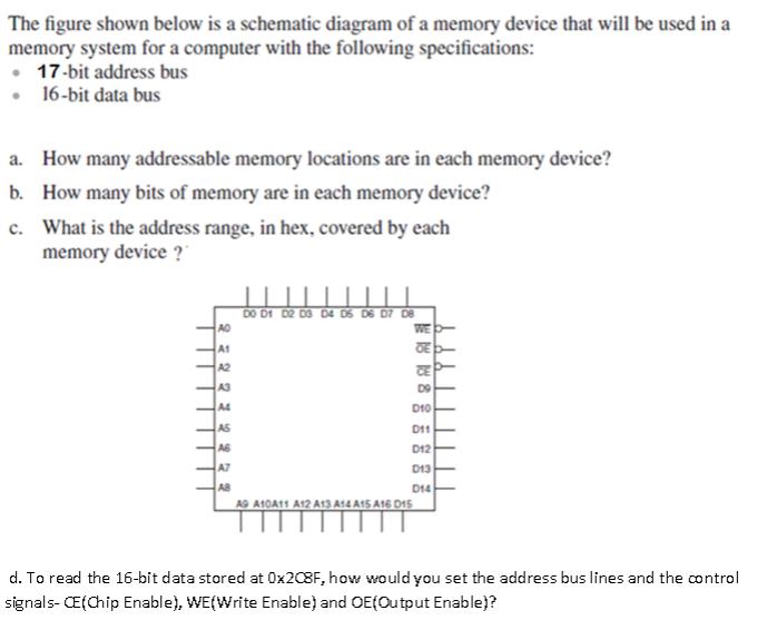
The figure shown below is a schematic diagram of a memory device that will be used in a memory system for a computer with

The figure shown below is a schematic diagram of a memory device that will be used in a memory system for a computer with the following specifications: . 17-bit address bus 16-bit data bus a. How many addressable memory locations are in each memory device? b. How many bits of memory are in each memory device? c. What is the address range, in hex, covered by each memory device? AO A1 A2 A3 AS A6 A7 DO 01 02 03 04 05 06 07 08 TE 8 D10 011 D12 013 D14 A9 A10A11 A12 A13 A14 A15 A16 D15 d. To read the 16-bit data stored at 0x2C8F, how would you set the address bus lines and the control signals- CE(Chip Enable), WE(Write Enable) and OE(Output Enable)?
Step by Step Solution
There are 3 Steps involved in it
Step: 1

Get Instant Access to Expert-Tailored Solutions
See step-by-step solutions with expert insights and AI powered tools for academic success
Step: 2

Step: 3

Ace Your Homework with AI
Get the answers you need in no time with our AI-driven, step-by-step assistance
Get StartedRecommended Textbook for
Systems analysis and design
Authors: kenneth e. kendall, julie e. kendall
8th Edition
135094909, 013608916X, 9780135094907, 978-0136089162
Students also viewed these Computer Network questions
Question
Answered: 1 week ago
Question
Answered: 1 week ago
Question
Answered: 1 week ago
Question
Answered: 1 week ago
Question
Answered: 1 week ago
Question
Answered: 1 week ago
Question
Answered: 1 week ago
Question
Answered: 1 week ago
Question
Answered: 1 week ago
Question
Answered: 1 week ago
Question
Answered: 1 week ago
Question
Answered: 1 week ago
Question
Answered: 1 week ago
Question
Answered: 1 week ago
Question
Answered: 1 week ago
Question
Answered: 1 week ago
Question
Answered: 1 week ago
Question
Answered: 1 week ago
Question
Answered: 1 week ago
Question
Answered: 1 week ago
Question
Answered: 1 week ago
Question
Answered: 1 week ago
View Answer in SolutionInn App


