Question
The formation of a silicon oxide (SiO2) thin film on a silicon (Si) wafer surface is an important step in the fabrication of solid-state microelectronic
The formation of a silicon oxide (SiO2) thin film on a silicon (Si) wafer surface is an important step in the fabrication of solid-state microelectronic devices. A thin film of SiO2 serves as a barrier to dopant diffusion or as a dielectric insulator to isolate various devices being formed on the wafer. In one common process, silicon is oxidized by exposure to oxygen (O2) gas at temperatures above 700C through this very fast chemical reaction: Si(s) + O2(g) SiO2(s).

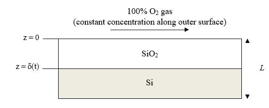
Molecular O2 dissolves into the SiO2 solid, diffuses through the SiO2 film, and then reacts with Si at the Si/SiO2 interface as shown in the figure above. Assume that the diffusion of O2 through the SiO2 film limits the oxidation process. Use the quasi- steady state assumption to develop a model to predict the thickness of the SiO2 layer (d) as a function of time at 1000C. The density of solid SiO2 (rB) is 2.27 g/cm3, and the molecular weight of SiO2 (MB) is 60 g/mol. The molecular diffusion coefficient of O2 in SiO2 (DAB) is 2.7 x 10⁻⁹ cm2/s at 1000C. The maximum solubility of O2 in SiO2 (CAs) is 9.6 x 10⁻⁸ mol O2/cm3 solid at 1000C and 1 atm O2 partial pressure. What is the thickness of the film, d, at 10 hours?
Answer is 0.22 mm, need step by step
100%O2 gas (constant concentration along outer surface)Step by Step Solution
There are 3 Steps involved in it
Step: 1

Get Instant Access to Expert-Tailored Solutions
See step-by-step solutions with expert insights and AI powered tools for academic success
Step: 2

Step: 3

Ace Your Homework with AI
Get the answers you need in no time with our AI-driven, step-by-step assistance
Get Started


