Answered step by step
Verified Expert Solution
Question
1 Approved Answer
the last figure is very important :( The purpose of this project is to design a sequential digital circuit that receives three 4- bit 2's


the last figure is very important :(
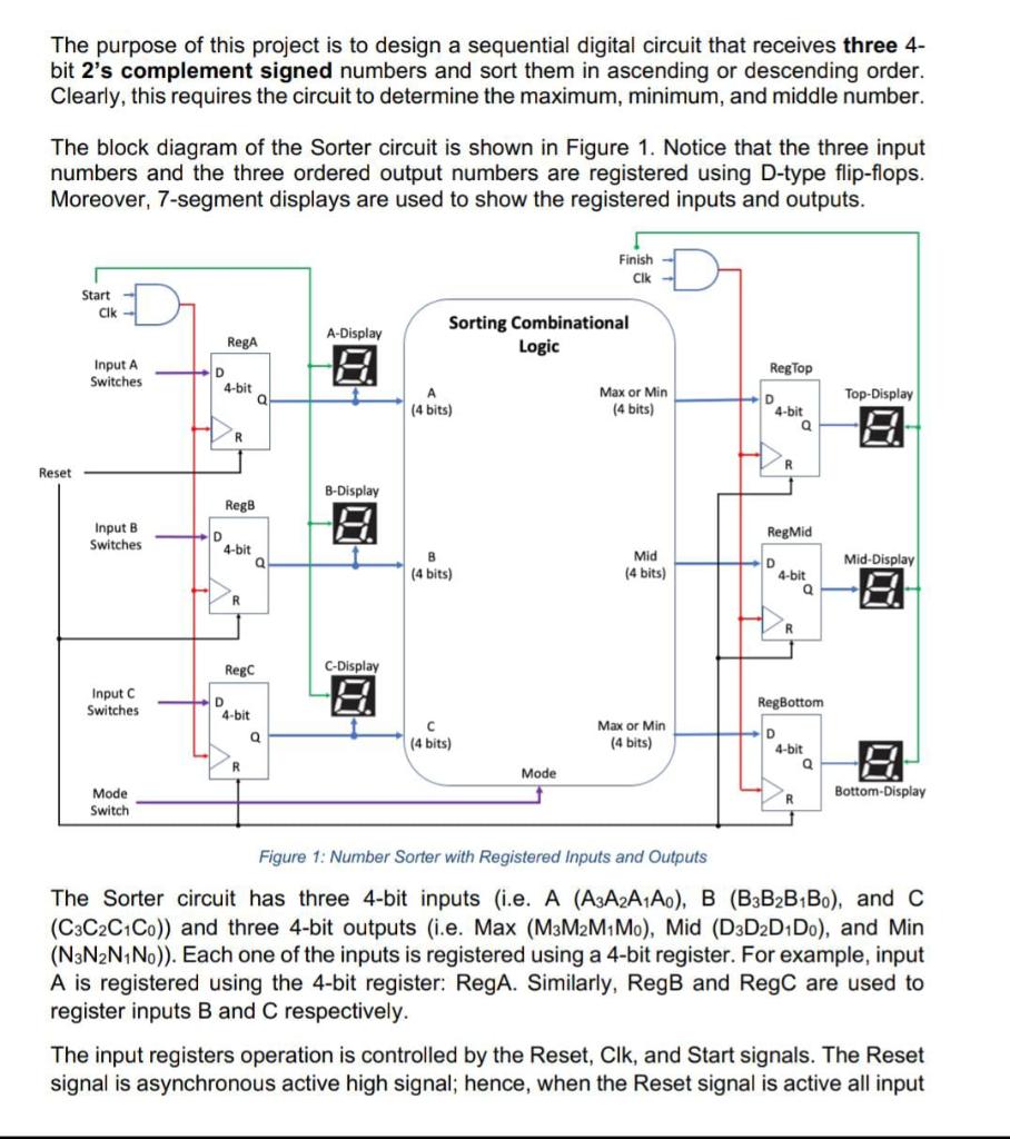
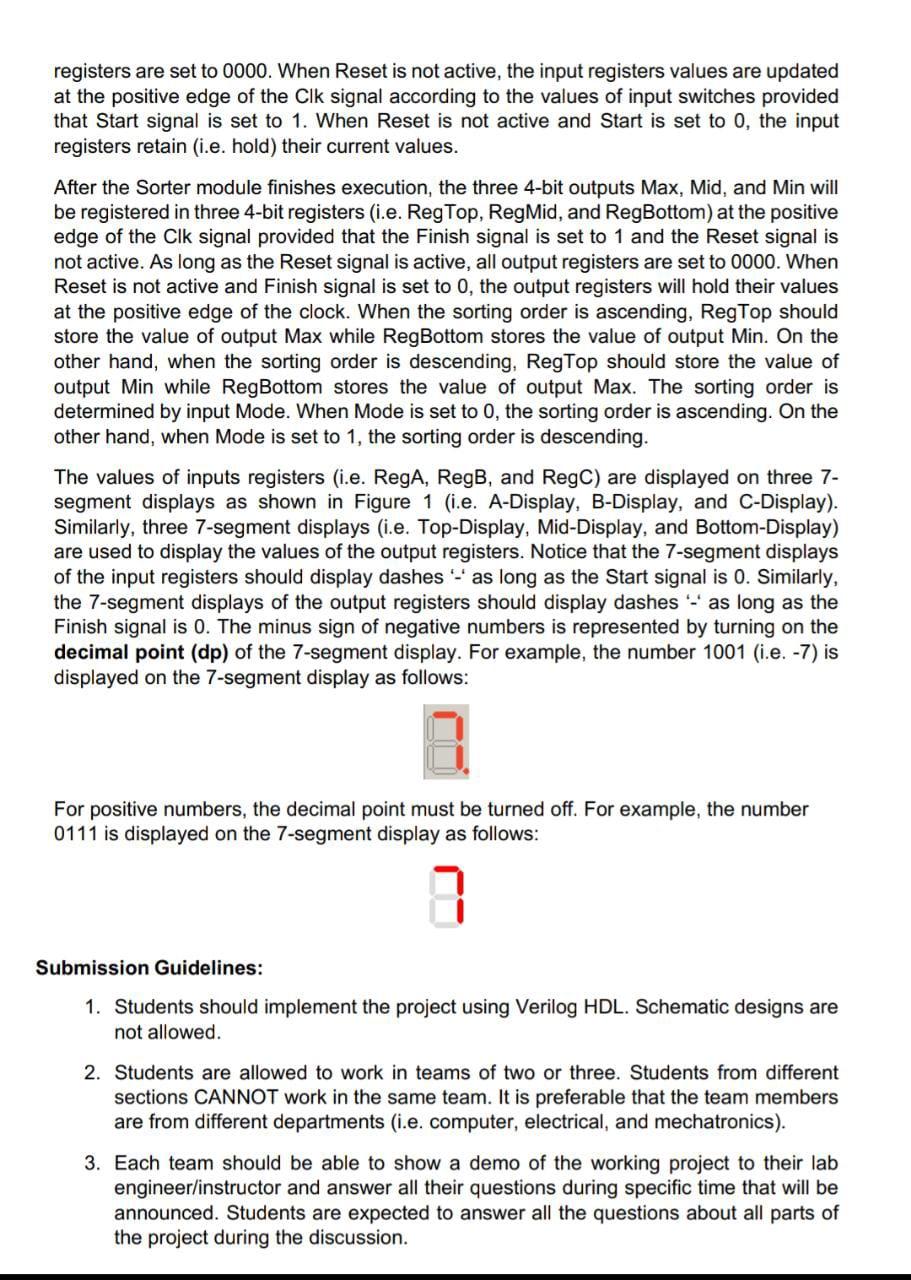
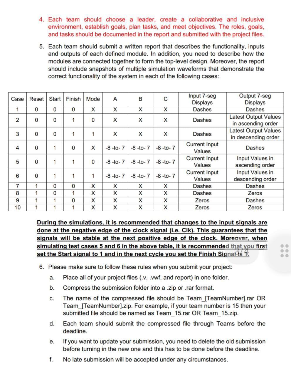
The purpose of this project is to design a sequential digital circuit that receives three 4- bit 2's complement signed numbers and sort them in ascending or descending order. Clearly, this requires the circuit to determine the maximum, minimum, and middle number. The block diagram of the Sorter circuit is shown in Figure 1. Notice that the three input numbers and the three ordered output numbers are registered using D-type flip-flops. Moreover, 7-segment displays are used to show the registered inputs and outputs. Finish Clk Start Clk A-Display Rega Sorting Combinational Logic Input A Reg Top Switches D 4-bit a A (4 bits) Max or Min (4 bits) Top-Display D 4-bit Q R R Reset B-Display RegB Input B Switches A RegMid D 4-bit a Mid (4 bits) B (4 bits) Mid-Display D 4-bit . R --- Regc C-Display Input C Switches A D 4-bit RegBottom Q (4 bits) Max or Min (4 bits) D 4-bit Q A R Mode Bottom-Display Mode Switch R Figure 1: Number Sorter with Registered Inputs and Outputs The Sorter circuit has three 4-bit inputs (ie. A (A3A2A1Ao), B (B3B2B-Bo), and C (C3C2C1Co)) and three 4-bit outputs (i.e. Max (M3M2M1 Mo), Mid (D3D2D-Do), and Min (N3N2N1No)). Each one of the inputs is registered using a 4-bit register. For example, input A is registered using the 4-bit register: Rega. Similarly, RegB and RegC are used to register inputs B and C respectively. The input registers operation is controlled by the Reset, Clk, and Start signals. The Reset signal is asynchronous active high signal; hence, when the Reset signal is active all input registers are set to 0000. When Reset is not active, the input registers values are updated at the positive edge of the Clk signal according to the values of input switches provided that Start signal is set to 1. When Reset is not active and Start is set to O, the input registers retain (i.e. hold) their current values. After the Sorter module finishes execution, the three 4-bit outputs Max, Mid, and Min will be registered in three 4-bit registers (i.e. Reg Top, RegMid, and RegBottom) at the positive edge of the Clk signal provided that the Finish signal is set to 1 and the Reset signal is not active. As long as the Reset signal is active, all output registers are set to 0000. When Reset is not active and Finish signal is set to O, the output registers will hold their values at the positive edge of the clock. When the sorting order is ascending, Reg Top should store the value of output Max while RegBottom stores the value of output Min. On the other hand, when the sorting order is descending, RegTop should store the value of output Min while RegBottom stores the value of output Max. The sorting order is determined by input Mode. When Mode is set to O, the sorting order is ascending. On the other hand, when Mode is set to 1, the sorting order is descending. The values of inputs registers (i.e. Rega, Regs, and RegC) are displayed on three 7- segment displays as shown in Figure 1 (i.e. A-Display, B-Display, and C-Display). Similarly, three 7-segment displays (i.e. Top-Display, Mid-Display, and Bottom-Display) are used to display the values of the output registers. Notice that the 7-segment displays of the input registers should display dashes - as long as the Start signal is 0. Similarly, the 7-segment displays of the output registers should display dashes - as long as the Finish signal is 0. The minus sign of negative numbers is represented by turning on the decimal point (dp) of the 7-segment display. For example, the number 1001 (i.e. -7) is displayed on the 7-segment display as follows: For positive numbers, the decimal point must be turned off. For example, the number 0111 is displayed on the 7-segment display as follows: Submission Guidelines: 1. Students should implement the project using Verilog HDL. Schematic designs are not allowed. 2. Students are allowed to work in teams of two or three. Students from different sections CANNOT work in the same team. It is preferable that the team members are from different departments (i.e. computer, electrical, and mechatronics). 3. Each team should be able to show a demo of the working project to their lab engineer/instructor and answer all their questions during specific time that will be announced. Students are expected to answer all the questions about all parts of the project during the discussion. 4. Each team should choose a leader, create a collaborative and inclusive environment, establish goals, plan tasks, and meet objectives. The roles, goals, and tasks should be documented in the report and submitted with the project files. 5. Each team should submit a written report that describes the functionality, inputs and outputs of each defined module. In addition, you need to describe how the modules are connected together to form the top-level design. Moreover, the report should include snapshots of multiple simulation waveforms that demonstrate the correct functionality of the system in each of the following cases: Case Reset Start Finish Mode B Input 7-seg Displays Dashes 1 0 0 0 X 2 0 0 1 0 X X Dashes Output 7-seg Displays Dashes Latest Output Values in ascending order Latest Output Values in descending order Dashes 3 0 0 1 1 x X Dashes 4 0 1 0 -8-to-7-8-to-7 -8-to-7 or 0 1 1 0 -8-to-7-8-to-7 -8-to-7 6 0 0 1 1 1 -8-to-7 -8 -to-7 -8-to-7 Current Input Values Current Input Values Current Input Values Dashes Dashes Zeros Zeros Input Values in ascending order Input Values in descending order Dashes Zeros Dashes Zeros 0 0 7 8 1 1 XXI Ic 1Step by Step Solution
There are 3 Steps involved in it
Step: 1

Get Instant Access to Expert-Tailored Solutions
See step-by-step solutions with expert insights and AI powered tools for academic success
Step: 2

Step: 3

Ace Your Homework with AI
Get the answers you need in no time with our AI-driven, step-by-step assistance
Get Started


