Answered step by step
Verified Expert Solution
Question
1 Approved Answer
The purpose of this project is to demonstrate the use of Boolean logic and build basic circuits. Note that this lab assignment is a

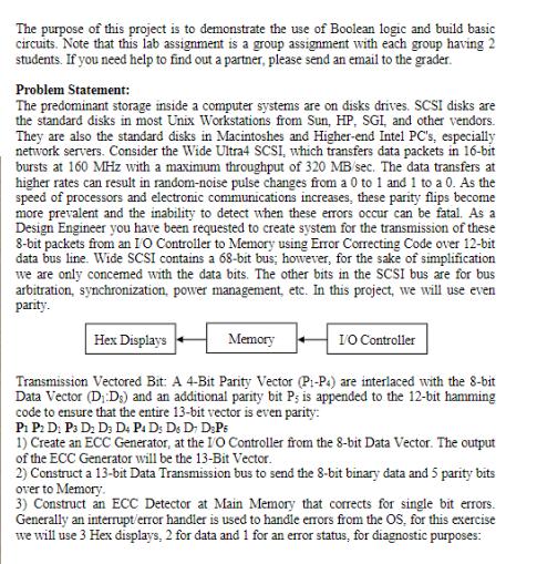
The purpose of this project is to demonstrate the use of Boolean logic and build basic circuits. Note that this lab assignment is a group assignment with each group having 2 students. If you need help to find out a partner, please send an email to the grader. Problem Statement: The predominant storage inside a computer systems are on disks drives. SCSI disks are the standard disks in most Unix Workstations from Sun, HP, SGI, and other vendors. They are also the standard disks in Macintoshes and Higher-end Intel PC's, especially network servers. Consider the Wide Ultra4 SCSI, which transfers data packets in 16-bit bursts at 160 MHz with a maximum throughput of 320 MB/sec. The data transfers at higher rates can result in random-noise pulse changes from a 0 to 1 and 1 to a 0. As the speed of processors and electronic communications increases, these parity flips become more prevalent and the inability to detect when these errors occur can be fatal. As a Design Engineer you have been requested to create system for the transmission of these 8-bit packets from an IO Controller to Memory using Error Correcting Code over 12-bit data bus line. Wide SCSI contains a 68-bit bus; however, for the sake of simplification we are only concerned with the data bits. The other bits in the SCSI bus are for bus arbitration, synchronization, power management, etc. In this project, we will use even parity. Hex Displays I/O Controller Transmission Vectored Bit: A 4-Bit Parity Vector (P-P4) are interlaced with the 8-bit Data Vector (D Ds) and an additional parity bit Ps is appended to the 12-bit hamming code to ensure that the entire 13-bit vector is even parity: P1 P2 D: P3 D D3 D4 P4 Ds Ds Dr DzPs 1) Create an ECC Generator, at the I/O Controller from the 8-bit Data Vector. The output of the ECC Generator will be the 13-Bit Vector. 2) Construct a 13-bit Data Transmission bus to send the 8-bit binary data and 5 parity bits over to Memory. 3) Construct an ECC Detector at Main Memory that corrects for single bit errors. Generally an interrupt/error handler is used to handle errors from the OS, for this exercise we will use 3 Hex displays, 2 for data and 1 for an error status, for diagnostic purposes: Memory
Step by Step Solution
★★★★★
3.44 Rating (157 Votes )
There are 3 Steps involved in it
Step: 1
Designing an Error Correcting Code ECC system for transmission of 8bit packets is a complex task that involves multiple components including an ECC Ge...
Get Instant Access to Expert-Tailored Solutions
See step-by-step solutions with expert insights and AI powered tools for academic success
Step: 2

Step: 3

Ace Your Homework with AI
Get the answers you need in no time with our AI-driven, step-by-step assistance
Get Started


