

Answered step by step
Verified Expert Solution
Question
1 Approved Answer
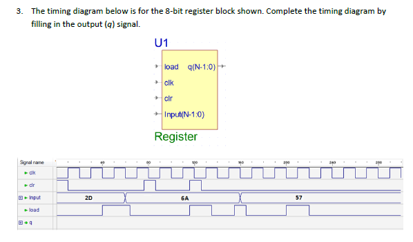
The timing diagram below is for the 8-bit register block shown. Complete the timing diagram by filling in the output (q) signal. 3. U1 load
Step by Step Solution
There are 3 Steps involved in it
Step: 1

Get Instant Access to Expert-Tailored Solutions
See step-by-step solutions with expert insights and AI powered tools for academic success
Step: 2

Step: 3
Ace Your Homework with AI
Get the answers you need in no time with our AI-driven, step-by-step assistance
Get Started
AWS Certified Database Study Guide Specialty DBS-C01 Exam
Authors: Matheus Arrais, Rene Martinez Bravet, Leonardo Ciccone, Angie Nobre Cocharero, Erika Kurauchi, Hugo Rozestraten
1st Edition
1119778956, 978-1119778950