Answered step by step
Verified Expert Solution
Question
1 Approved Answer
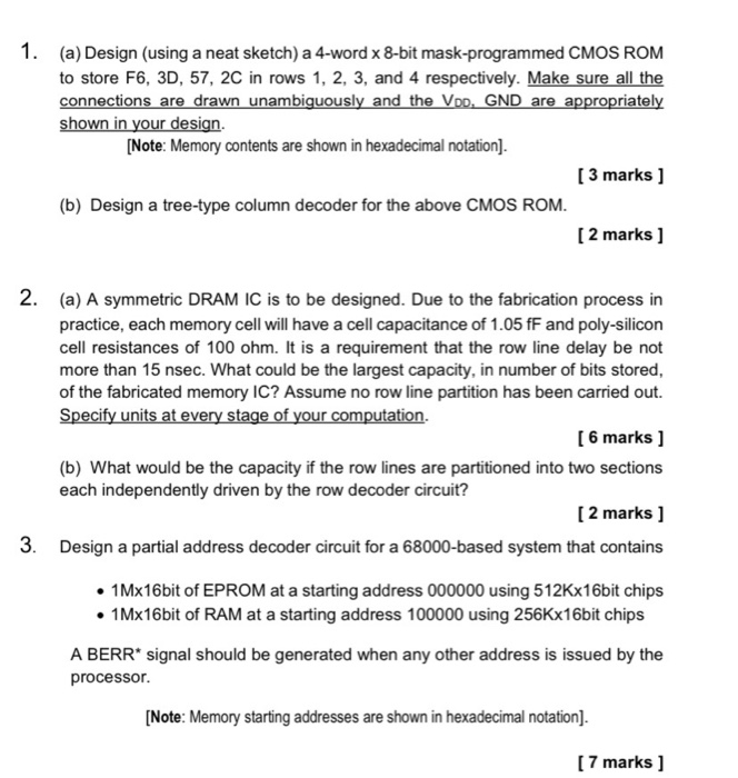
They havent posted the answers and i want to know how to do these please 1. (a) Design (using a neat sketch) a 4-word x
They havent posted the answers and i want to know how to do these please 
1. (a) Design (using a neat sketch) a 4-word x 8-bit mask-programmed CMOS ROM to store F6, 3D, 57, 2C in rows 1, 2, 3, and 4 respectively. Make sure all the connections are drawn unambiguously and the Vpo. GND are appropriately shown in your design. (Note: Memory contents are shown in hexadecimal notation). [3 marks ] (b) Design a tree-type column decoder for the above CMOS ROM. [2 marks] 2. (a) A symmetric DRAM IC is to be designed. Due to the fabrication process in practice, each memory cell will have a cell capacitance of 1.05 ff and poly-silicon cell resistances of 100 ohm. It is a requirement that the row line delay be not more than 15 nsec. What could be the largest capacity, in number of bits stored, of the fabricated memory IC? Assume no row line partition has been carried out. Specify units at every stage of your computation. [6 marks ] (b) What would be the capacity if the row lines are partitioned into two sections each independently driven by the row decoder circuit? [2 marks] 3. Design a partial address decoder circuit for a 68000-based system that contains 1Mx16bit of EPROM at a starting address 000000 using 512Kx16bit chips 1Mx16bit of RAM at a starting address 100000 using 256Kx16bit chips A BERR* signal should be generated when any other address is issued by the processor. [Note: Memory starting addresses are shown in hexadecimal notation). [7 marks ] 
Step by Step Solution
There are 3 Steps involved in it
Step: 1

Get Instant Access to Expert-Tailored Solutions
See step-by-step solutions with expert insights and AI powered tools for academic success
Step: 2

Step: 3

Ace Your Homework with AI
Get the answers you need in no time with our AI-driven, step-by-step assistance
Get Started


