Answered step by step
Verified Expert Solution
Link Copied!

Question

1 Approved Answer

times (since you are building a 4-bit adder). To re-emphasize, 'adder gate' is your top-level Complete the code, compile it and assign pins using switches
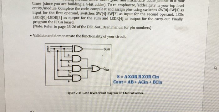
image text in transcribed
times (since you are building a 4-bit adder). To re-emphasize, 'adder gate' is your top-level Complete the code, compile it and assign pins using switches sW[o]-SW[3] as input for the first operand, switches SW[4]-SW[7] as input for the second operand, LEDs LEDR[0]-LEDR(3] as output for the sum and LEDR[4] as output for the carry-out. Finally program the FPGA board. (Note: Refer to page 25-26 of the DE1-SoC.User, manual for pin numbers) Validate and demonstrate the functionality of your circuit. Sum Cout Cout AB + ACin +BCin Figure 7.1: Gate-level circuit diagram of 1-bit Full adder

Step by Step Solution

There are 3 Steps involved in it

Step: 1

blur-text-image

Get Instant Access to Expert-Tailored Solutions

See step-by-step solutions with expert insights and AI powered tools for academic success

Step: 2

blur-text-image

Step: 3

blur-text-image

Ace Your Homework with AI

Get the answers you need in no time with our AI-driven, step-by-step assistance

Get Started

Recommended Textbook for

Advances In Databases 11th British National Conference On Databases Bncod 11 Keele Uk July 7 9 1993 Proceedings Lncs 696

Authors: Michael F. Worboys ,Anna F. Grundy

1993rd Edition

3540569219, 978-3540569213

More Books

Students also viewed these Databases questions

Question

Identify the influence of social media on political communication

Answered: 1 week ago