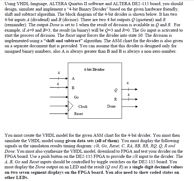
Using VHDL language, ALTERA Quartus II software and ALTERA DE2-115 board, you should design, simulate and implement a "4-bit Binary Divider" based on the given hardware friendly shift and subtract algorithm. The block diagram of the 4-bit divider is shown below. It has two 4-bit inputs A (dividend) and B (divisor). There are two 4-bit outputs Q (quotient) and R (remainder). The output Done is set to 1 when the result of division is available in Q and R. For example, if A-9 and B-3, the result (in binary) will be Q-3 and R-0. The Go input is activated to start the process of division. The Reset input forces the divider into state SO. The division is implemented using a "shift and subtract" algorithm. The ASM chart for the divider is also given on a separate document that is provided. You can assume that this divider is designed only for unsigned binary numbers, also A is always greater than B and B is always a non-zero number 4-bit Divider 4 4 4 Clock Reset You must create the VHDL model for the given ASM chart for the 4-bit divider. You must then simulate the VHDL model using given data sets (all of them). You must display the following signals in the simulation results timing diagram: clk, Go, Reset, C, RA, RB, RR, RQ, Q, R and Done. You must also synthesize the VHDL model, download to FPGA and test your divider on the FPGA board. Use a push button on the DE2-115 FPGA to provide the clk input to the divider. The A, B, Go and Reset inputs should be controlled by toggle switches on the DE2-115 board. You must display the Done output on an LED and the result (Q and R) as a single digit decimal values on two seven segment displays on the FPGA board. You also need to show coded states on other LEDs. Using VHDL language, ALTERA Quartus II software and ALTERA DE2-115 board, you should design, simulate and implement a "4-bit Binary Divider" based on the given hardware friendly shift and subtract algorithm. The block diagram of the 4-bit divider is shown below. It has two 4-bit inputs A (dividend) and B (divisor). There are two 4-bit outputs Q (quotient) and R (remainder). The output Done is set to 1 when the result of division is available in Q and R. For example, if A-9 and B-3, the result (in binary) will be Q-3 and R-0. The Go input is activated to start the process of division. The Reset input forces the divider into state SO. The division is implemented using a "shift and subtract" algorithm. The ASM chart for the divider is also given on a separate document that is provided. You can assume that this divider is designed only for unsigned binary numbers, also A is always greater than B and B is always a non-zero number 4-bit Divider 4 4 4 Clock Reset You must create the VHDL model for the given ASM chart for the 4-bit divider. You must then simulate the VHDL model using given data sets (all of them). You must display the following signals in the simulation results timing diagram: clk, Go, Reset, C, RA, RB, RR, RQ, Q, R and Done. You must also synthesize the VHDL model, download to FPGA and test your divider on the FPGA board. Use a push button on the DE2-115 FPGA to provide the clk input to the divider. The A, B, Go and Reset inputs should be controlled by toggle switches on the DE2-115 board. You must display the Done output on an LED and the result (Q and R) as a single digit decimal values on two seven segment displays on the FPGA board. You also need to show coded states on other LEDs