Question
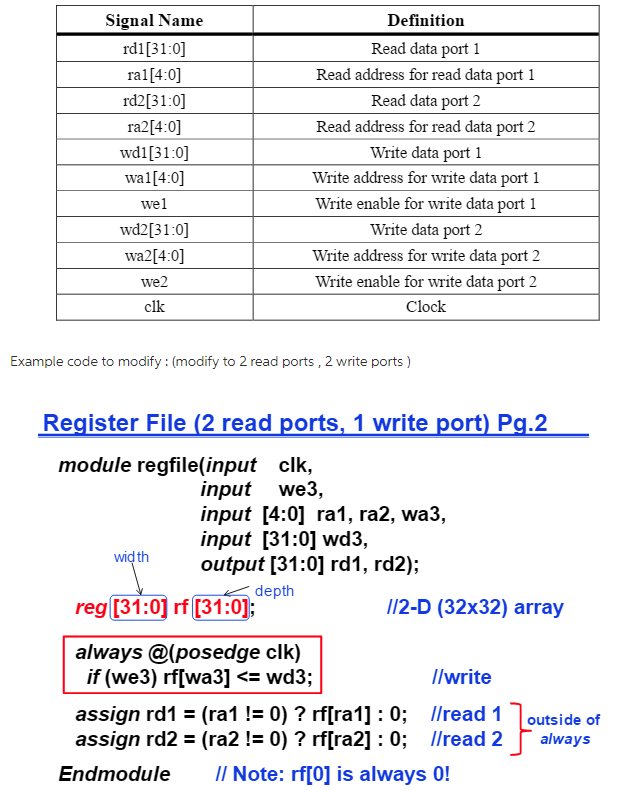
(Verilog 2001 HDL) Design and functionally verify a 32x32 register file (module name regfile2) with 2 read ports and 2 write ports, following the I/O
(Verilog 2001 HDL) Design and functionally verify a 32x32 register file (module name regfile2) with 2 read ports and 2 write ports, following the I/O signal naming given below:

Use a self-checking testbench for functional verification of the register file.
Please make sure that all write and read ports operate properly. Also test that all locations in the register file can be written to and read from. You do not have to go through all possible inputs for each register file location.
Specific Requirement: Your testbench should have a decent coverage, particularly, you need to test the corner case in which both read addresses and one of the write addresses are the same, and the corresponding write enable is asserted (e.g., ra1 = ra2 = wa1 and we1 = 1, or ra1 = ra2 = wa2 and we2 = 1), and explain your observation.
Note: The situation of simultaneous write into the same register should never be allowed!
Signal Name rd1[31:0] ra1[4:0] rd2[31:0] ra204:0] wd1 [31:0] wa1[4:0] wel wd2[31:0] wa2[4:0] we2 Definition Read data port 1 Read address for read data port 1 Read data port 2 Read address for read data port 2 Write data port1 Write address for write data port 1 Write enable for write data port 1 Write data port2 Write address for write data port 2 Write enable for write data port 2 Clock Example code to modify : (modify to 2 read ports, 2 write ports ) Register File (2 read ports, 1 write port) Pa.2 module regfile(input clk, input we3, input [4:0] ra1, ra2, wa3, input [31:0] wd3, thoutput [31:0] rd1, rd2); depth //2-D (32x32) array reg [31:0] rf (31:0] always @(posedge clk) assign rd1 (ra1 ! 0)? rf[ra1]: 0 read 1 outside of //write assign rd2 (ra2!E 0)? rf[ra2]: 0; Ilread 2always EndmoduleII Note: rf0] is always O! Signal Name rd1[31:0] ra1[4:0] rd2[31:0] ra204:0] wd1 [31:0] wa1[4:0] wel wd2[31:0] wa2[4:0] we2 Definition Read data port 1 Read address for read data port 1 Read data port 2 Read address for read data port 2 Write data port1 Write address for write data port 1 Write enable for write data port 1 Write data port2 Write address for write data port 2 Write enable for write data port 2 Clock Example code to modify : (modify to 2 read ports, 2 write ports ) Register File (2 read ports, 1 write port) Pa.2 module regfile(input clk, input we3, input [4:0] ra1, ra2, wa3, input [31:0] wd3, thoutput [31:0] rd1, rd2); depth //2-D (32x32) array reg [31:0] rf (31:0] always @(posedge clk) assign rd1 (ra1 ! 0)? rf[ra1]: 0 read 1 outside of //write assign rd2 (ra2!E 0)? rf[ra2]: 0; Ilread 2always EndmoduleII Note: rf0] is always OStep by Step Solution
There are 3 Steps involved in it
Step: 1

Get Instant Access to Expert-Tailored Solutions
See step-by-step solutions with expert insights and AI powered tools for academic success
Step: 2

Step: 3

Ace Your Homework with AI
Get the answers you need in no time with our AI-driven, step-by-step assistance
Get Started


