Answered step by step
Verified Expert Solution
Question
1 Approved Answer
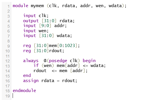
[Verilog] Write the testbench to simulate the behaviours of module mymem : To describe an inferred RAM in Verilog, there have some following signals: clk:
[Verilog] Write the testbench to simulate the behaviours of module mymem:
- To describe an inferred RAM in Verilog, there have some following signals:
- clk: clock;
- rdata: output read data from RAM;
- address: read/write address;
- wdata: data that will be write to RAM;
- wen: allow to the wdata write to RAM at address.
- Describe RAM as an array.
- Read/write activity have to be triggered by a clock. Reset/Set is not allowed when using RAM.
- The direct output of RAM have to be captured by a register before assign to rdata. Otherwise, RAM is not infered
To know your RAM design inferred successfully. Synthesize then look at "Design Run" tab in Vivado, if the value at the column "BRAM" or "URAM" is higher than 0, it means there are RAM that is inferrred.

Step by Step Solution
There are 3 Steps involved in it
Step: 1

Get Instant Access to Expert-Tailored Solutions
See step-by-step solutions with expert insights and AI powered tools for academic success
Step: 2

Step: 3

Ace Your Homework with AI
Get the answers you need in no time with our AI-driven, step-by-step assistance
Get Started


