Answered step by step
Verified Expert Solution
Question
1 Approved Answer
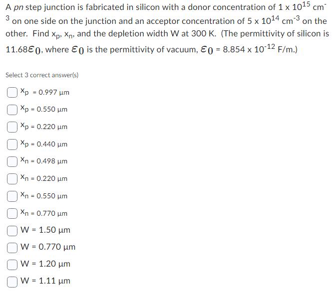
3 A pn step junction is fabricated in silicon with a donor concentration of 1 x 1015 cm on one side on the junction

3 A pn step junction is fabricated in silicon with a donor concentration of 1 x 1015 cm on one side on the junction and an acceptor concentration of 5 x 1014 cm 3 on the other. Find Xp, Xn, and the depletion width W at 300 K. (The permittivity of silicon is 11.68 0, where is the permittivity of vacuum, &0 = 8.854 x 10⁻¹² F/m.) Select 3 correct answer(s) |Xp = 0.997 m Xp = 0.550 m Xp = 0.220 m Xp = 0.440 m Xn = 0.498 m Xn = 0.220 m Xn = 0.550 m n = 0.770 m W = 1.50 m W = 0.770 m W = 1.20 m W = 1.11 m
Step by Step Solution
★★★★★
3.49 Rating (159 Votes )
There are 3 Steps involved in it
Step: 1
To find xp and xn we need to use the intrinsic carrier concentrations and the donor and acceptor concentrations The intrinsic carrier concentration in silicon is about 108 x 1010 cm3 at room temperatu...
Get Instant Access to Expert-Tailored Solutions
See step-by-step solutions with expert insights and AI powered tools for academic success
Step: 2

Step: 3

Ace Your Homework with AI
Get the answers you need in no time with our AI-driven, step-by-step assistance
Get Started


