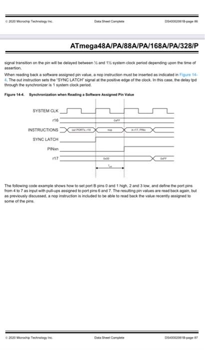
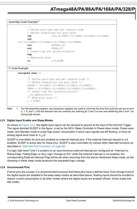
Write a program in C to blink the on board LED of the Xplained board at a rate of about once per second. It is not necessary to use interrupts or timers. Do not use any predefined functions. You should configure the port pin as a high side output and then be able to set the state of the port pin. Follow the instructions in Section 14.2 of the data sheet. Follow the schematic of the Xplained board ATmega328P_Xplained_Mini_design_documentation_release - in order to determine which port pin to activate. Note the following - port pins are bit wise controlled by powers of 2. To activate port pin 0 - set the port to 1(20); To activate port pin 1 - set the port to 2(21); To activate port pin 2 - set the port to 4(22); 14.2 Ports as General Digital VO The ports are bl-diecsonal wO ports with opsonal internal pult-ups. Figure 14.2 shows a functional descripton of one llo-poit pin, here genericaly caled Pxn. Vigure 14-7 Note: 1. WFx, WPr, WDx, RRx, RPx, and RDx are cemmon to at pins within the same pert ckNo sLEEP, and PUD are corminen to all porta. 14.2.1 Configuring the Pin Each port pin consists of three register bits: DDxh, PORTxn, and PINxt. As shown in 'Fugster Descriplion' on poge 100, the DDxn biss are accessed at the DDFK IIO address, the POFTin bits at the PORTX IO address, and the PiNm bits at the PINx WO addrest. The DDxn bat in the DDRx Register selects the drection of this pin. If DDxa is witten logic one, Pxn is configured as an output pin. If DDxn is written logic zero, Pan is configured as an input pin. If PORTxn is writien logic one when the pin is configured as an input pin, the pult-sp resistor is activated. To saikh the pull-up resistor off, PORTxn has to be writien logic zero or the pin has to be configured as an output pin. The port pins are tri-staled when reset constion becomes active, even if no clocks are running. If PORTxn is weitten logic one when the pin is configured as an output pin, the port pin is driven high (one), if PORTxn is wetten logic zero when the pin is configured as an cutput pin, the pod pin is driven low (zeeo). 14.2.2 Toggling the Pin Writing a logic one to PINxn toggles the value of POFT Xn, independent on the value of DDFEn. Nobe than the SBI instruction can be used to toggle one single bt in a port. 14.2.3 Switching Between Input and Output When swilching between tristale (DDxn, PORTxn) =0600 ) and output high (DOm. PORT intermediate state with either gult-up enabled (DOm. PORTXn) = 0601) or eutput low (YDDxn, PORT 1} ) 0610) must occur. Nonsally, the pul-up enabled state is tully acceptable, as a high-impedance environment will not notice the ditterence betwoen a streng high driver and a pult-up. If this is not the case. the PuD bit in the MCUCR Register can be set to disable all pulleups in all ports. signe transition on the pin wil be delayed between Yk and 1% system clock. period depending upon the time of assertion. When reading back a software aseigned pin value, a nop instruction must be ineerled as indicated in figure 14 4, The out iastruction sets the -SYNC LATCH signal at fhe pesitive edge of the dock. In this case, the delay lpd through the synchronizer is 1 system cleck period. Figure 14-4. Svechronizatien when Readina a Sottware Aasianed Pin Value The following oode example shows how to set port 8 pins 0 and 1 high, 2 and 3 low, and define the port pirs. from 4 to 7 as input with pult-ups aseigned to port pins 6 and 7 . The resulting pin values are read beck agait, but as prevously discussed, a nop instruction is included to be able to read back the value recertly assigned le sombl of the pint. 2.5 Digital Input Enable and Sleep Modes As shown in Figure 14-2, the digital input signal can be clamped to ground at the input of the Schmitt Trigger. The signal denoted SLEEP in the figure, is set by the MCU Sleep Controller in Power-down mode, Power-5ave mode, and Standby mode to avoid high power consumption if some input signals are left floating, or have an analog signal level close to Vcc/2. SLEEP is overridden for port pins enabled as extemal interrupt pins. If the extemal interrupt request is not enabled, SLEEP is active also for these pins. SLEEP is also overridden by various other altemate functions as described in "Alternate Port Functions" on page 89 , If a logic high level ("one") is present on an asynchronous external interrupt pin configured as "Internupt on Rising Edge, Falling Edge, or Any Logic Change on Pin" while the external interrupt is not enabled, the corresponding External Interrupt Flag will be set when resuming from the above mentioned Sleep mode, as the clamping in these sleep mode produces the requested logic change. ,2.6 Unconnected Pins If some pins are unused, it is recommended to ensure that these pins have a defined level, Even though most of the digital inputs are disabled in the deep sleep modes as described above, floating inputs should be avoided to reduce current consumption in all other modes where the digital inputs are enabled (Reset, Active mode and Idle mode)


