In many systems various delays are required. In this project you will create a four bit variable delay circuit. The circuit will implement one


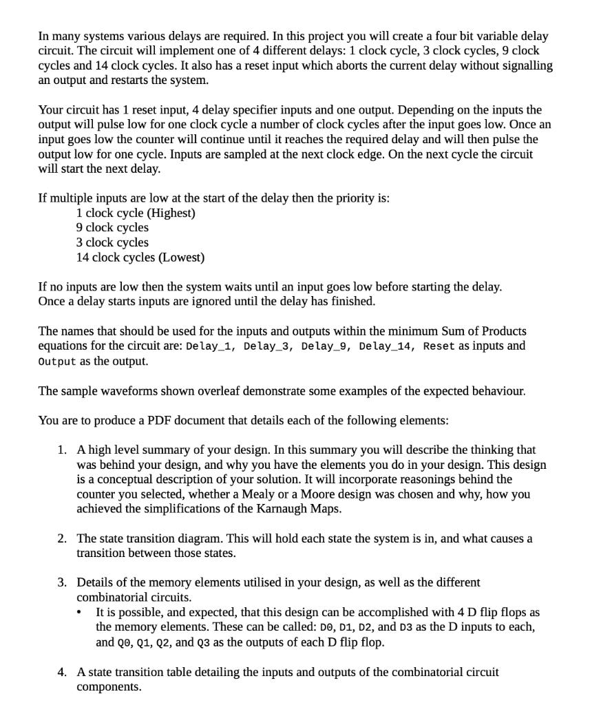
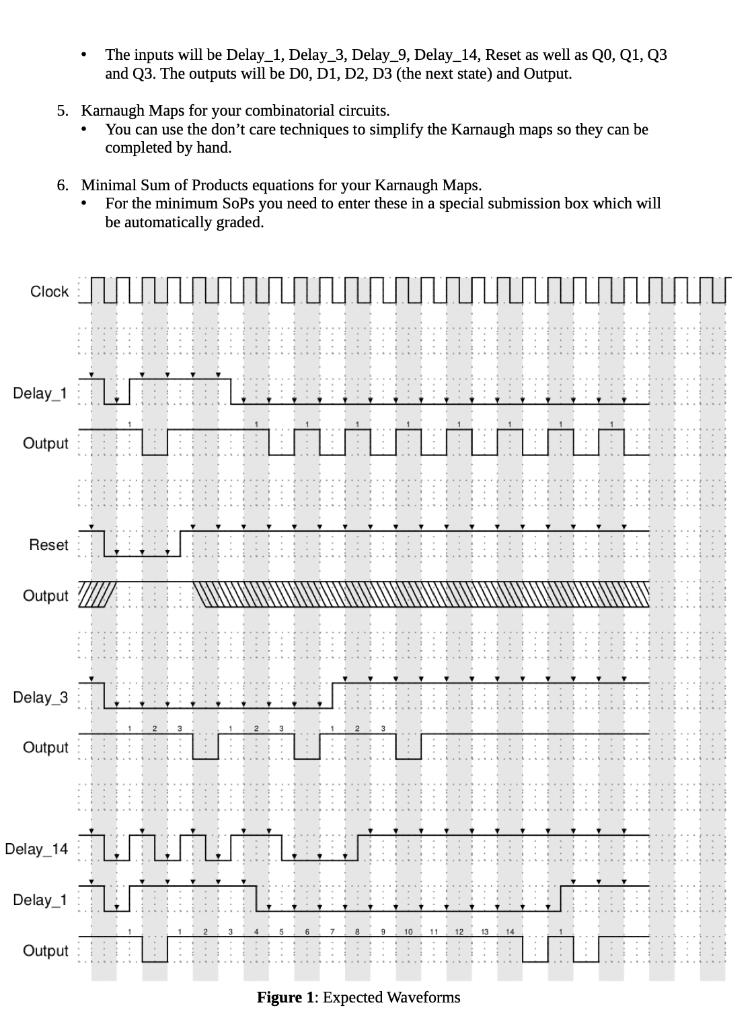
In many systems various delays are required. In this project you will create a four bit variable delay circuit. The circuit will implement one of 4 different delays: 1 clock cycle, 3 clock cycles, 9 clock cycles and 14 clock cycles. It also has a reset input which aborts the current delay without signalling an output and restarts the system. Your circuit has 1 reset input, 4 delay specifier inputs and one output. Depending on the inputs the output will pulse low for one clock cycle a number of clock cycles after the input goes low. Once an input goes low the counter will continue until it reaches the required delay and will then pulse the output low for one cycle. Inputs are sampled at the next clock edge. On the next cycle the circuit will start the next delay. If multiple inputs are low at the start of the delay then the priority is: 1 clock cycle (Highest) 9 clock cycles 3 clock cycles 14 clock cycles (Lowest) If no inputs are low then the system waits until an input goes low before starting the delay. Once a delay starts inputs are ignored until the delay has finished. The names that should be used for the inputs and outputs within the minimum Sum of Products equations for the circuit are: De lay_ 1, Delay 3, Delay_9, Delay_14, Reset as inputs and Output as the output. The sample waveforms shown overleaf demonstrate some examples of the expected behaviour. You are to produce a PDF document that details each of the following elements: 1. A high level summary of your design. In this summary you will describe the thinking that was behind your design, and why you have the elements you do in your design. This design is a conceptual description of your solution. It will incorporate reasonings behind the counter you selected, whether a Mealy or a Moore design was chosen and why, how you achieved the simplifications of the Karnaugh Maps. 2. The state transition diagram. This will hold each state the system is in, and what causes a transition between those states. 3. Details of the memory elements utilised in your design, as well as the different combinatorial circuits. . It is possible, and expected, that this design can be accomplished with 4 D flip flops as the memory elements. These can be called: D0, D1, D2, and D3 as the D inputs to each, and Qo, Q1, Q2, and Q3 as the outputs of each D flip flop. 4. A state transition table detailing the inputs and outputs of the combinatorial circuit components. 5. Karnaugh Maps for your combinatorial circuits. You can use the don't care techniques to simplify the Karnaugh maps so they can be completed by hand. 6. Minimal Sum of Products equations for your Karnaugh Maps. For the minimum SoPs you need to enter these in a special submission box which will be automatically graded. Clock: Delay 1 Output Reset Output Delay 3 Output Delay 14 Delay 1 The inputs will be Delay_1, Delay_3, Delay_9, Delay_14, Reset as well as Q0, Q1, Q3 and Q3. The outputs will be D0, D1, D2, D3 (the next state) and Output. Output . 8 9 10 11 m 12 Figure 1: Expected Waveforms 13 14 uuuuu
Step by Step Solution
There are 3 Steps involved in it
Step: 1
This project involves designing a circuit to implement a multidelay system The task is to create a state machine that can output different delays base...
See step-by-step solutions with expert insights and AI powered tools for academic success
Step: 2

Step: 3

Ace Your Homework with AI
Get the answers you need in no time with our AI-driven, step-by-step assistance
Get Started


