

Question: Consider the PMOS common-source circuit in Figure P4.24 with transistor parameters (V_{T P}=-2 mathrm{~V}) and (lambda=0), and circuit parameters (R_{D}=R_{L}=) (10 mathrm{k} Omega). (a) Determine
Consider the PMOS common-source circuit in Figure P4.24 with transistor parameters \(V_{T P}=-2 \mathrm{~V}\) and \(\lambda=0\), and circuit parameters \(R_{D}=R_{L}=\) \(10 \mathrm{k} \Omega\).
(a) Determine the values of \(K_{p}\) and \(R_{S}\) such that \(V_{S D Q}=6 \mathrm{~V}\).
(b) Determine the resulting value of \(I_{D Q}\) and the small-signal voltage gain.
(c) Can the values of \(K_{p}\) and \(R_{S}\) from part (a) be changed to achieve a larger voltage gain, while still meeting the requirements of part (a)?
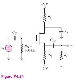
Ca +5 V Rs RG= 100 CC2 C's Ri Ro Figure P4.24 -5 V
Step by Step Solution
3.42 Rating (158 Votes )
There are 3 Steps involved in it

Get step-by-step solutions from verified subject matter experts