The operation of a digital system is coordinated and controlled by a periodic waveform called a clock.
Question:
The operation of a digital system is coordinated and controlled by a periodic waveform called a clock. The clock waveform provides a standard timing reference to maintain synchronization between signal processing results that are generated asynchronously. Because of differences in digital circuit delays, there must be agreed-upon instants of time at which circuit outputs can be treated as valid inputs to other circuits.
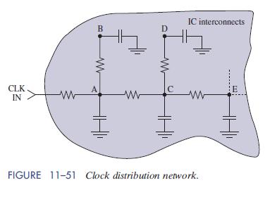
Figure 11–51 shows a section of the clock distribution network in an integrated circuit. In this network, the clock waveform is generated at one point and distributed to other on-chip locations by interconnections that can be modeled as lumped resistors and capacitors. Clock distribution

problems arise when the RC circuit delays at different locations are not the same.
This delay dispersion is called clock skew, defined as the time difference between a clock edge at one location and the corresponding edge at another location.
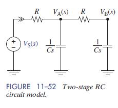
To qualitatively calculate a clock skew, we will find the step responses in the RC circuit in Figure 11–52. The input VSðsÞ is a unit step function that simulates the leading edge of a clock pulse. The resulting step responses VAðsÞ and VBðsÞ represent the clock waveforms at points A and B in a clock distribution network. To find the step responses, we use the following s-domain node-voltage equations

which indicates that the circuit has simple poles at s = −0:382=RC and s = −2:618=RC.
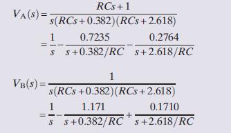
Using the circuit determinant and a unit step input, we can easily solve the node equations for VAðsÞ and VBðsÞ:

From these we obtain the time-domain step responses as


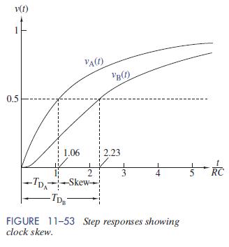
These two responses are plotted in Figure 11–53. For a unit step input, both responses have a final value of unity. Using the definition of step response delay time given in Example 11–12 (time required to reach 50% of the final value), we see that TDA =1:06=RC and TDB =2:23=RC The delay time skew is Delay Skew=TDB −TDA =1:17=RC The clock distribution problem is not that the RC elements representing the interconnects produce time delay, but that delays are not all the same. Ideally, digital devices at different locations should operate on their respective digital inputs at exactly the same instant of time. Erroneous results may occur when the clock pulse defining that instant does not arrive at all locations at the same time. Minimizing clock skew is one of the major constraints on the design of the clock distribution network in large-scale integrated circuits.

Step by Step Answer:

The Analysis And Design Of Linear Circuits
ISBN: 9781119235385
8th Edition
Authors: Roland E. Thomas, Albert J. Rosa, Gregory J. Toussaint


