

Undesired Ringing , A digital clock has become corrupted by a ringing (undesired oscillations) as shown in
Question:
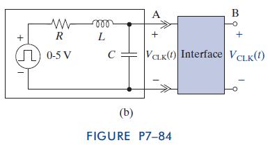
Undesired Ringing , A digital clock has become corrupted by a ringing (undesired oscillations) as shown in Figure P7–84(a). The unwanted oscillations can cause false triggers and must be reduced. The clock can be modeled as an RLC series circuit as shown in Figure P7–84
(b) with the voltage taken at node A. The parasitic capacitance is estimated at 0.01 mF and the Thevenin resistance at 330 V. Fromthe graph determine the inductance L. Design an interface circuit that significantly reduces the ringing without significantly reducing the rise time (the time it takes the pulse to go from low to high or vice-versa.) The transition must occur in less than 80 us and the ‘‘overshoot’’ (deviation from 0 or 5 V)
must be less than1V. Fromthe graph determine L. Then design a suitable interface to meet the output specifications. Use standard value components. Use OrCAD to validate your design.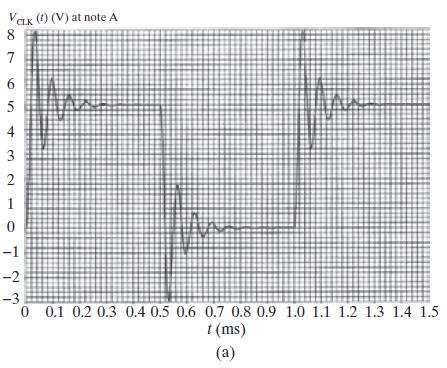
Step by Step Answer:

This question has not been answered yet.
You can Ask your question!

The Analysis And Design Of Linear Circuits
ISBN: 9781118214299
7th Edition
Authors: Roland E Thomas, Albert J Rosa, Gregory J Toussaint
