A tool used for fabricating semiconductor devices consists of a chuck (thick metallic, cylindrical disk) onto which
Question:
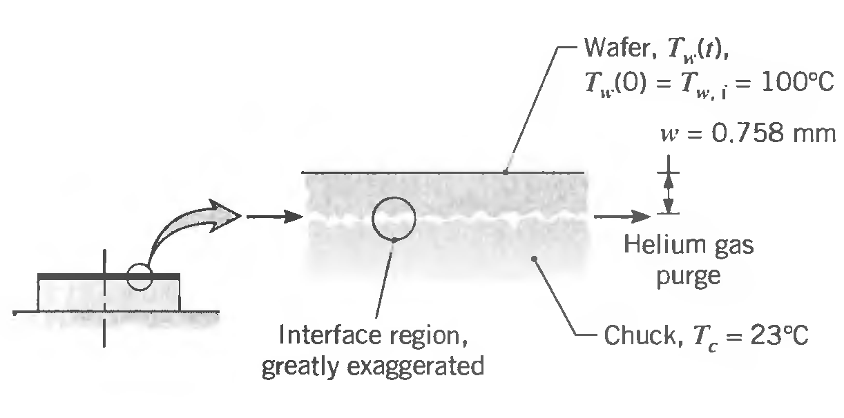
A tool used for fabricating semiconductor devices consists of a chuck (thick metallic, cylindrical disk) onto which a very thin silicon wafer (p = 2700 kg/m3 ∙ c = 875 J/kg ∙ K, k = 177 W/m ∙ K) is placed by a robotic arm. Once in position, an electric field in the chuck is energized, creating an electrostatic force that holds the wafer firmly to the chuck. To ensure a reproducible thermal contact resistance between the chuck and the wafer from cycle-to-cycle pressurized helium gas is introduced at the center of the chuck and flows (very slowly) radially outward between the asperities of the interface region.

An experiment has been performed under conditions for which the wafer, initially at a uniform temperature Tw,i = 100°C, is suddenly placed on the chuck, which is at a uniform and constant temperature Tc = 23°C. With the wafer in place, the electrostatic force and the helium gas flow are applied. After 15 seconds, the temperature of the wafer is determined to be 33°C. What is the thermal contact resistance Rt,c (m2 ∙ K/W) between the wafer and chuck? Will the value of Rt,c increase, decrease, or remain the same if air, instead of helium, is used as the purge gas?
Step by Step Answer:

Fundamentals of Heat and Mass Transfer
ISBN: 978-0471457282
6th Edition
Authors: Incropera, Dewitt, Bergman, Lavine


