

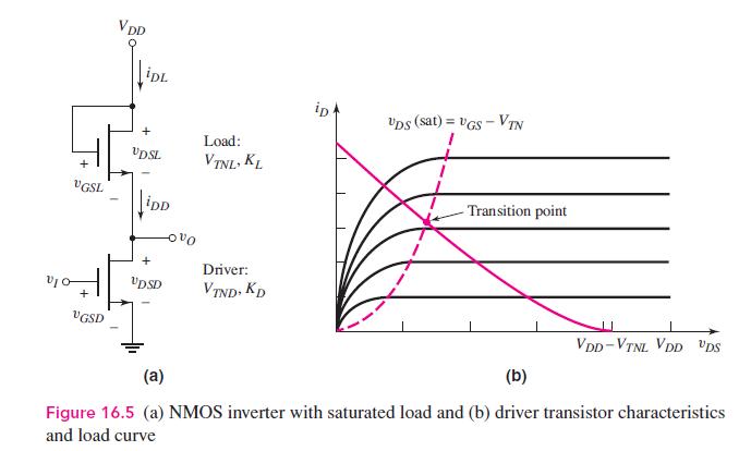
Consider the NMOS inverter with saturated load in Figure 16.5(a). Let (V_{D D}=3 mathrm{~V}). (a) Design the
Question:
Consider the NMOS inverter with saturated load in Figure 16.5(a). Let \(V_{D D}=3 \mathrm{~V}\).
(a) Design the circuit such that the power dissipation in the circuit is \(400 \mu \mathrm{W}\) and the output voltage is \(0.10 \mathrm{~V}\) when the input voltage is a logic 1.
(b) Determine the transition point of the driver transistor.
Fantastic news! We've Found the answer you've been seeking!
Step by Step Answer:

Answered By
Amit Choudhary
I'm new in this profession regarding online teaching but previously i used to teach students near my college. I am teaching on online platform since last year and got good support from the students. I'm teaching on platforms like chegg and vedantu and also at my home in free time.
1+ Reviews
10+ Question Solved
Related Book For 

Microelectronics Circuit Analysis And Design
ISBN: 9780071289474
4th Edition
Authors: Donald A. Neamen
Question Posted:
