

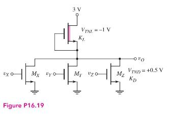
Consider the three-input NOR logic gate in Figure P16.19. The transistor parameters are (V_{T N L}=-1 mathrm{~V})
Question:
Consider the three-input NOR logic gate in Figure P16.19. The transistor parameters are \(V_{T N L}=-1 \mathrm{~V}\) and \(V_{T N D}=0.5 \mathrm{~V}\). The maximum value of \(v_{O}\) in its low state is to be \(0.1 \mathrm{~V}\).
(a) Determine \(K_{D} / K_{L}\).
(b) The maximum power dissipation in the NOR logic gate is to be \(0.1 \mathrm{~mW}\). Determine the width-to-length ratios of the transistors.
(c) Determine \(v_{O}\) when \(v_{X}=v_{Y}=\) \(v_{Z}=3 \mathrm{~V}\).
Fantastic news! We've Found the answer you've been seeking!
Step by Step Answer:

Answered By
Asim farooq
I have done MS finance and expertise in the field of Accounting, finance, cost accounting, security analysis and portfolio management and management, MS office is at my fingertips, I want my client to take advantage of my practical knowledge. I have been mentoring my client on a freelancer website from last two years, Currently I am working in Telecom company as a financial analyst and before that working as an accountant with Pepsi for one year. I also join a nonprofit organization as a finance assistant to my job duties are making payment to client after tax calculation, I have started my professional career from teaching I was teaching to a master's level student for two years in the evening.
My Expert Service
Financial accounting, Financial management, Cost accounting, Human resource management, Business communication and report writing. Financial accounting : • Journal entries • Financial statements including balance sheet, Profit & Loss account, Cash flow statement • Adjustment entries • Ratio analysis • Accounting concepts • Single entry accounting • Double entry accounting • Bills of exchange • Bank reconciliation statements Cost accounting : • Budgeting • Job order costing • Process costing • Cost of goods sold Financial management : • Capital budgeting • Net Present Value (NPV) • Internal Rate of Return (IRR) • Payback period • Discounted cash flows • Financial analysis • Capital assets pricing model • Simple interest, Compound interest & annuities
65+ Reviews
86+ Question Solved
Related Book For 

Microelectronics Circuit Analysis And Design
ISBN: 9780071289474
4th Edition
Authors: Donald A. Neamen
Question Posted:
