

Question: A BiCMOS Class AB output stage is shown in Fig. 5.43. Device parameters are β F (npn) = 80, β F (pnp) = 20, V
A BiCMOS Class AB output stage is shown in Fig. 5.43. Device parameters are βF(npn) = 80, βF(pnp) = 20, VBE(on)= 0.8 V, μpCox= 26 µA/V2, and Vt= ˆ’0.7 V.
(a) Calculate bias currents in all devices for Vo = 0.
(b) Calculate the positive and negative limits of Vo for RL = 200 Ω. Thus calculate the maximum average power that can be delivered to RL before clipping occurs.
(c) Use SPICE to check (a) and also to plot the complete dc transfer characteristic of the circuit from Vi to Vo. Also plot the waveforms of Ic1, Ic2, and Id2 for a sinusoidal output voltage at Vo of 2 V and then 4 V zero-to-peak. In the simulation, assume bipolar parameters as in Fig. 2.32 and MOS parameters as in Table 2.3 (apart from the values of βF and μpCox given above).
Figure 5.43:
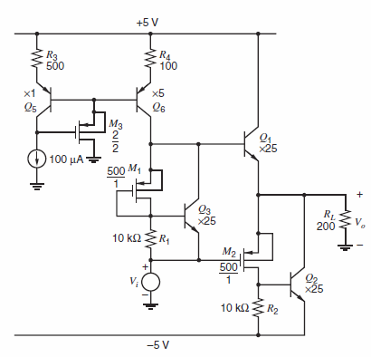
Fig. 2.32:
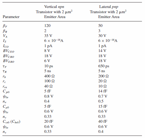
+5 V R3 500 RA 100 1 x5 O5 25 O 100 100 A 500 M4 25 RL Va 200 10 K2ER M2 500 02 x25 10 k2 R2 -5 V VIN 81-L Vertical npn Transistor with 2 um Emitter Area Lateral pnp Transistor with 2 m? Parameter Emitter Area Br VA Is Ico BVCEO BVCBO BVEBO 120 50 35 V 30 V 6 x 10-18A 1 pA 6 x 10-18A 1 pA 14 V 18 V 18 V 18 V 10 ps 5 ns 650 ps 5 ns TF TR 400 2 200 2 re 100 2 20 2 rex 40 2 10 2 5 fF 14 fF 0.8 V 0.7 V ne 0.4 0.5 5 fF 15 fF 0.6 V 0.6 V 0.33 0.33 Coo (Cho) 20 fF 40 fF 0.6 V 0.6 V 0.33 0.4 3.
Step by Step Solution
3.41 Rating (157 Votes )
There are 3 Steps involved in it
a Bias V o 0 I C5 100 A I C6 500 A I D3 I B5 I B6 600 A20 30 A I C3 500 80 420 A From KVL V GS... View full answer

Get step-by-step solutions from verified subject matter experts
Document Format (2 attachments)
1528_605d88e1b2cb3_686872.pdf
180 KBs PDF File
1528_605d88e1b2cb3_686872.docx
120 KBs Word File