

Question: Determine the input resistance, transconductance, output resistance, and maximum open-circuit voltage gain for the CS-CG circuit of Fig.3.38 if I D1 = I D2 =
Determine the input resistance, transconductance, output resistance, and maximum open-circuit voltage gain for the CS-CG circuit of Fig.3.38 if ID1 = ID2= 250 µA. Assume W/L=100, λ=0.1 V−1, and χ = 0.1. Use Table 2.2 for other parameters.
Fig. 3.38:
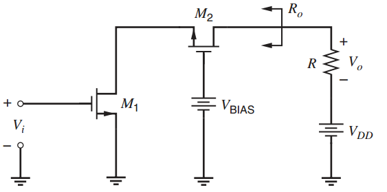
Table 2.2:
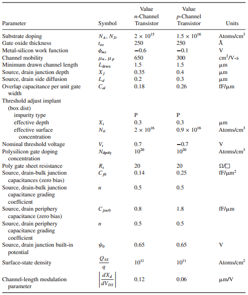
Ro M2 V. V BIAS VDD M1 V; Value Value n-Channel Transistor p-Channel Parameter Symbol Transistor Units Substrate doping Gate oxide thickness 1.5 x 10¹⁶ NA, Np 2 x 10⁵ Atoms/cm lox 250 250 Metal-silicon work function -0.6 -0.1 cm?/V-s Channel mobility Minimum drawn channel length Source, drain junction depth Source, drain side diffusion 650 300 Larwn X; 1.5 1.5 0.35 0.4 La 0.2 0.3 um Cal Overlap capacitance per unit gate width 0.18 0.26 fF/um Threshold adjust implant (box dist) impurity type effective depth 0.3 0.3 um effective surface Nsi 2 x 10¹⁶ 0.9 x 10¹⁶ Atoms/cm concentration Nominal threshold voltage Polysilicon gate doping V, 0.7 -0.7 Napoly 100 Atoms/cm concentration Poly gate sheet resistance Source, drain-bulk junction R, 20 20 0.14 0.25 fF/um? capacitances (zero bias) Source, drain-bulk junction capacitance grading 0.5 0.5 coefficient Source, drain periphery capacitance (zero bias) Source, drain periphery capacitance grading 0.8 1.8 fF/um 0.5 0.5 coefficient Source, drain junction built-in potential 0.65 0.65 Oss Surface-state density 10" 10" Atoms/cm PXP dV ps Channel-length modulation 0.12 0.06 m/V parameter
Step by Step Solution
3.46 Rating (169 Votes )
There are 3 Steps involved in it
R i 21 mAV R o g m2 g mb2 r ... View full answer

Get step-by-step solutions from verified subject matter experts
Document Format (2 attachments)
1528_605d88e1a8dfd_686770.pdf
180 KBs PDF File
1528_605d88e1a8dfd_686770.docx
120 KBs Word File