

Question: For the CMOS operational amplifier shown in Fig. 9.60, calculate the open-loop voltage gain, unity gain bandwidth, and slew rate. Assume the parameters of Table
For the CMOS operational amplifier shown in Fig. 9.60, calculate the open-loop voltage gain, unity gain bandwidth, and slew rate. Assume the parameters of Table 2.1 with Xd= 1 µm. Assume that the gate of M9is connected to the positive power supply and that the W/L of M9has been chosen to cancel the right half-plane zero. Compare your results with a SPICE simulation.
Fig. 9.60:
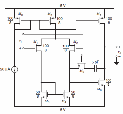
Table 2.1:
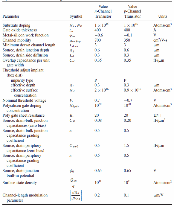
+5 V M8 M5 100 M7 100 100 8. Vi M1 100 M2 100 5 pF 20 M9 100 M6 50 50 M4 -5 V Value Value n-Channel p-Channel Parameter Symbol Transistor Transistor Units 1 x 10⁵ 1 x 10¹⁶ 400 Atoms/cm3 Substrate doping Gate oxide thickness NA, Np tex 400 Metal-silicon work function -0.6 -0.1 cm?/V-s Channel mobility Minimum drawn channel length Source, drain junction depth Source, drain side diffusion Overlap capacitance per unit gate width Threshold adjust implant (box dist) 700 350 Ldrwn X j 3 0.6 0.6 0.3 0.35 La 0.3 um Cd 0.35 Fm impurity type effective depth effective surface , Nsi 0.3 0.3 um 2 x 10¹⁶ 0.9 x 10¹⁶ Atoms/cm concentration Nominal threshold voltage Polysilicon gate doping V, 0.7 -0.7 Napoly 1020 1020 Atoms/cm concentration Poly gate sheet resistance Source, drain-bulk junction capacitances (zero bias) Source, drain-bulk junction capacitance grading R, 20 20 Cp 0.08 0.20 fF/um? 0.5 0.5 coefficient Source, drain periphery capacitance (zero bias) Source, drain periphery capacitance grading coefficient Cjawo 0.5 1.5 fF/um 0.5 0.5 0.65 0.65 Source, drain junction built-in potential Q ss Surface-state density 10" 10" Atoms/cm? dX4 Channel-length modulation 0.2 0.1 um/V dVps parameter
Step by Step Solution
3.34 Rating (169 Votes )
There are 3 Steps involved in it
L eff L 2Ld Xd 8 203 1 64 I D 20 A for m g m 5 m 7 m 6 I D 10 ... View full answer

Get step-by-step solutions from verified subject matter experts
Document Format (2 attachments)
1528_605d88e1c78d2_687096.pdf
180 KBs PDF File
1528_605d88e1c78d2_687096.docx
120 KBs Word File