

Question: (a) Use logic simulation to verify that the circuits described in Example 3-18 implement the BCDtoseven-segment converter correctly. (b) Design the converter assuming that the
(a) Use logic simulation to verify that the circuits described in Example 3-18 implement the BCD–to–seven-segment converter correctly.
(b) Design the converter assuming that the unused input combinations (minterms 10–15) can be don’t cares rather than 0s. Simulate your design and compare it to your simulation from part (a).
Example 3-18
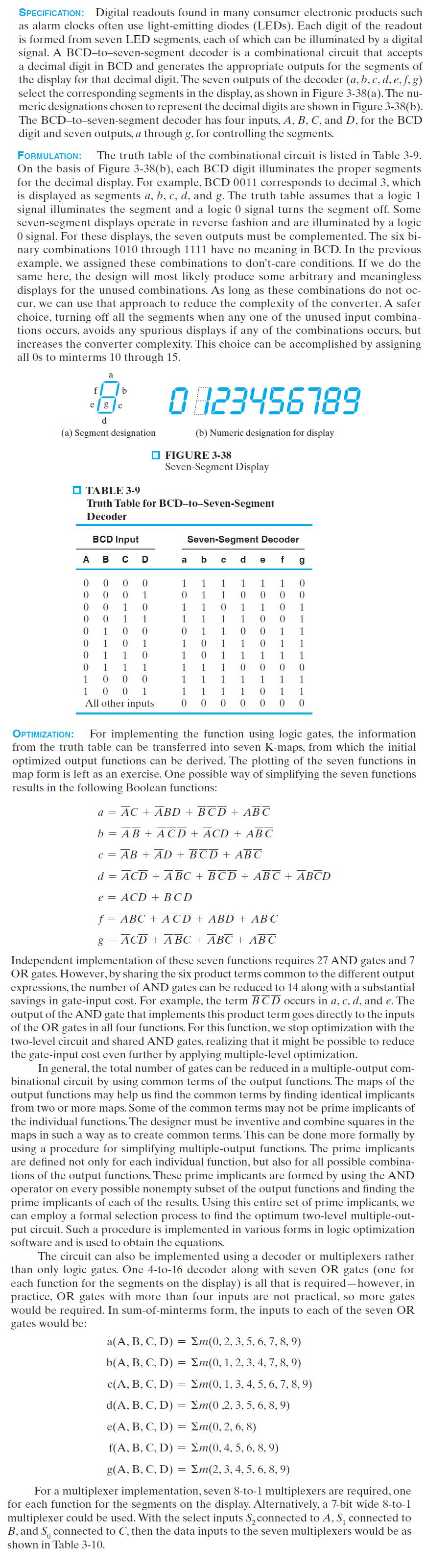
SPECIFICATION: Digital readouts found in many consumer electronic products such as alarm clocks often use light-emitting diodes (LEDs). Each digit of the readout is formed from seven LED segments, each of which can be illuminated by a digital signal. A BCD-to-seven-segment decoder is a combinational circuit that accepts a decimal digit in BCD and generates the appropriate outputs for the segments of the display for that decimal digit. The seven outputs of the decoder (a, b, c, d, e, f, g) select the corresponding segments in the display, as shown in Figure 3-38(a). The nu- meric designations chosen to represent the decimal digits are shown in Figure 3-38(b). The BCD-to-seven-segment decoder has four inputs, A, B, C, and D, for the BCD digit and seven outputs, a through g, for controlling the segments. FORMULATION: The truth table of the combinational circuit is listed in Table 3-9. On the basis of Figure 3-38(b), each BCD digit illuminates the proper segments for the decimal display. For example, BCD 0011 corresponds to decimal 3, which is displayed as segments a, b, c, d, and g. The truth table assumes that a logic 1 signal illuminates the segment and a logic 0 signal turns the segment off. Some seven-segment displays operate in reverse fashion and are illuminated by a logic 0 signal. For these displays, the seven outputs must be complemented. The six bi- nary combinations 1010 through 1111 have no meaning in BCD. In the previous example, we assigned these combinations to don't-care conditions. If we do the same here, the design will most likely produce some arbitrary and meaningless displays for the unused combinations. As long as these combinations do not oc- cur, we can use that approach to reduce the complexity of the converter. A safer choice, turning off all the segments when any one of the unused input combina- tions occurs, avoids any spurious displays if any of the combinations occurs, but increases the converter complexity. This choice can be accomplished by assigning all Os to minterms 10 through 15. f e g d (a) Segment designation a A 0 0 b TABLE 3-9 Truth Table for BCD-to-Seven-Segment Decoder BCD Input 0 0 0 0 0 0 0 0 0 B C D 0 0 1 1 0 0 1 0 1 0823456789 (b) Numeric designation for display 1 0 1 1 1 1 0 0 0 1 0 0 1 All other inputs FIGURE 3-38 Seven-Segment Display a b Seven-Segment Decoder d e f 1 0 1 1 1 1 0 0 0 1 1 1 0 0 0 0 0 1 1 1 0 0 0 = g 0 1 1 1 1 1 1 0 0 1 1 1 1 0 1 1 0 0 0 0 OPTIMIZATION: For implementing the function using logic gates, the information from the truth table can be transferred into seven K-maps, from which the initial optimized output functions can be derived. The plotting of the seven functions in map form is left as an exercise. One possible way of simplifying the seven functions results in the following Boolean functions: a = = AC + ABD + BCD + ABC b = AB+ ACD + ACD + ABC c = AB + AD + BCD + ABC d = ACD + ABC + BCD + ABC + ABCD e = ACD + BCD f = ABC + ACD + ABD + ABC g= ACD + ABC + ABC + ABC Independent implementation of these seven functions requires 27 AND gates and 7 OR gates. However, by sharing the six product terms common to the different output expressions, the number of AND gates can be reduced to 14 along with a substantial savings in gate-input cost. For example, the term BCD occurs in a, c, d, and e. The output of the AND gate that implements this product term goes directly to the inputs of the OR gates in all four functions. For this function, we stop optimization with the two-level circuit and shared AND gates, realizing that it might be possible to reduce the gate-input cost even further by applying multiple-level optimization. In general, the total number of gates can be reduced in a multiple-output com- binational circuit by using common terms of the output functions. The maps of the output functions may help us find the common terms by finding identical implicants from two or more maps. Some of the common terms may not be prime implicants of the individual functions. The designer must be inventive and combine squares in the maps in such a way as to create common terms. This can be done more formally by using a procedure for simplifying multiple-output functions. The prime implicants are defined not only for each individual function, but also for all possible combina- tions of the output functions. These prime implicants are formed by using the AND operator on every possible nonempty subset of the output functions and finding the prime implicants of each of the results. Using this entire set of prime implicants, we can employ a formal selection process to find the optimum two-level multiple-out- put circuit. Such a procedure is implemented in various forms in logic optimization software and is used to obtain the equations. The circuit can also be implemented using a decoder or multiplexers rather than only logic gates. One 4-to-16 decoder along with seven OR gates (one for each function for the segments on the display) is all that is required-however, in practice, OR gates with more than four inputs are not practical, so more gates would be required. In sum-of-minterms form, the inputs to each of the seven OR gates would be: a(A, B, C, D) = m(0, 2, 3, 5, 6, 7, 8, 9) b(A, B, C, D) Em(0, 1, 2, 3, 4, 7, 8, 9) c(A, B, C, D) = m(0, 1, 3, 4, 5, 6, 7, 8, 9) d(A, B, C, D) = m(0,2, 3, 5, 6, 8, 9) e(A, B, C, D) = m(0, 2, 6, 8) f(A, B, C, D) = m(0, 4, 5, 6, 8, 9) g(A, B, C, D) = Em (2, 3, 4, 5, 6, 8, 9) For a multiplexer implementation, seven 8-to-1 multiplexers are required, one for each function for the segments on the display. Alternatively, a 7-bit wide 8-to-1 multiplexer could be used. With the select inputs S connected to A, S, connected to B, and S connected to C, then the data inputs to the seven multiplexers would be as shown in Table 3-10.
Step by Step Solution
3.34 Rating (148 Votes )
There are 3 Steps involved in it
a sop ABDABCABDAB... View full answer

Get step-by-step solutions from verified subject matter experts