Answered step by step
Verified Expert Solution
Question
1 Approved Answer
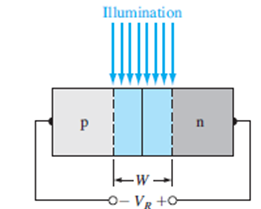
Consider, as shown in Figure, a uniformly doped silicon pn junction at T = 300 K with impurity doping concentrations of N a = N
Consider, as shown in Figure, a uniformly doped silicon pn junction at T = 300 K with impurity doping concentrations of N a = N d = 5 x 10 15 cm -3 and minority carrier lifetimes of T n0 = T p0 = T O = 10-7 S. A reverse-biased voltage of VR = 10 V is applied. A light source is incident only on the space charge region, producing an excess carrier generation rate of g' = 4 x 10 19 cm -3 s-1. Calculate the generation current density.

Illumination |_w_ -O-V +0 n
Step by Step Solution
★★★★★
3.47 Rating (177 Votes )
There are 3 Steps involved in it
Step: 1
Write the expression for the builtin potential across the semiconductor device V bi Here V t is the ...
Get Instant Access to Expert-Tailored Solutions
See step-by-step solutions with expert insights and AI powered tools for academic success
Step: 2

Step: 3

Document Format ( 2 attachments)
6095e576d34c9_26369.pdf
180 KBs PDF File
6095e576d34c9_26369.docx
120 KBs Word File
Ace Your Homework with AI
Get the answers you need in no time with our AI-driven, step-by-step assistance
Get Started


